Showing posts with label amplifier. Show all posts

Saturday, September 28, 2013

9V HEADPHONE AMPLIFIER NE5534 ELECTRONIC DIAGRAM

9V HEADPHONE AMPLIFIER NE5534 ELECTRONIC DIAGRAM

I have Used it with Sennheiser 465s and achieved ear-splitting volume. The amplifier is ideal as a booster for power-conserving stereo sources Such as portable CD players and for interfacing with passive EQ networks Such as tone controls or a headphone acoustic simulator.
Continue Reading[...]

Wednesday, June 12, 2013

10Watt Audio Amplifier with Bass boost circuit


Circuit diagram

parts list 

P1_________________22K   Log.Potentiometer (Dual-gang for stereo)
P2________________100K   Log.Potentiometer (Dual-gang for stereo)
R1________________820R   1/4W Resistor
R2,R4,R8____________4K7  1/4W Resistors
R3________________500R   1/2W Trimmer Cermet
R5_________________82K   1/4W Resistor
R6,R7______________47K   1/4W Resistors
R9_________________10R   1/2W Resistor
R10__________________R22   4W Resistor (wirewound)

C1,C8_____________470nF   63V Polyester Capacitor
C2,C5_____________100µF   25V Electrolytic Capacitors
C3,C4_____________470µF   25V Electrolytic Capacitors
C6_________________47pF   63V Ceramic or Polystyrene Capacitor
C7_________________10nF   63V Polyester Capacitor
C9________________100nF   63V Polyester Capacitor

D1______________1N4148    75V 150mA Diode

IC1_____________NE5532    Low noise Dual Op-amp

Q1_______________BC547B   45V 100mA NPN Transistor
Q2_______________BC557B   45V 100mA PNP Transistor
Q3_______________TIP42A   60V 6A    PNP Transistor
Q4_______________TIP41A   60V 6A    NPN Transistor

J1__________________RCA audio input socket

Power supply circuit


                                  Circuit diagram
Parts 

R11_________________1K5  1/4W Resistor

C10,C11__________4700µF   25V Electrolytic Capacitors

D2________________100V 4A Diode bridge
D3________________5mm. Red LED

T1________________220V Primary, 12 + 12V Secondary 24-30VA Mains transformer

PL1_______________Male Mains plug

SW1_______________SPST Mains switch .Electronics Circuit Application


Continue Reading[...]

Sunday, April 21, 2013

Circuit Guards Amplifier Outputs Against Overvoltage

A universal requirement for automotive electronics is that any device with direct connections to the wiring harness must be able to withstand shorts to the battery voltage. Though brutal, this requirement is necessary for reliability and for safety. One example of the need for this protection is an audio amplifier that produces indicator noises in the automotive interior. Though operating from a voltage of 3.3 or 5V, which is lower than the battery voltage, the amplifier must be able to stand off the full battery voltage. 
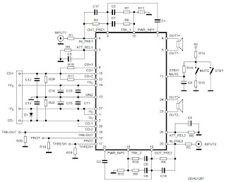
Circuit diagram :
amplifier outputs against overvoltage
Figure 1 : This output circuit provides continuose protection against overvoltge faults

You can also use a protection network appropriate for these amplifiers for other automotive circuits (Figure 1). A dual N-channel MOSFET disconnects the amplifier’s outputs from the wiring harness in response to a high-voltage condition on either output. The MOSFETs, Q1A and Q1B, are normally on; zener diode D4 and its bias components drive the MOSFETs’ gates to approximately 11V. Dual diode D3 provides a diode-OR connection to the dc voltage on each output, thereby producing a voltage that controls the output of shunt regulator IC2. The circuitry protects IC1, a 1.4W Class AB amplifier suitable for audible warnings and indications for the automotive electronics. 

During normal operation, the amplifier outputs’ dc components are at one-half of the VCC supply—2.5V in this case, for which VCC is 5V. The 11V gate drive fully enhances the MOSFETs, and the shunt-regulator output is off because its feedback input, Pin 5, is below its internal 0.6V threshold. If either output exceeds 5V, current flows through D3 into the R5/R6 divider, pulling the feedback terminal above its threshold. The shunt-regulator output then pulls the MOSFET-gate voltage from 11V almost to ground, which blocks high voltage from the amplifier by turning off the MOSFETs. The MOSFETs easily withstand the continuous output voltage, and the circuit returns to normal operation when you remove the short. Because the circuit does not respond instantaneously, zener diodes D1 and D2 provide protection at the beginning of a fault condition.
Figure 2. Figure 2. In Figure 1, one of U1s two audio outputs (top trace) is protected when its external terminal accidentally contacts an 18V supply voltage (2nd trace).

The waveforms of Figure 2 represent an operating circuit. One of the amplifier’s outputs (Trace 1) is a 1-kHz sine wave biased at a dc voltage of 2.5V. Trace 2 is the signal on the wire harness. It also starts as a 1-kHz sine wave biased at a 2.5V-dc voltage, but, at 200 µsec, it shorts to an 18V supply. Trace 3 is the shunt regulator’s output, initially biased at 11V but pulled to ground in response to the overvoltage condition. Trace 4 is current in the wire harness. Initially a sine wave, this current drops to zero in response to the overvoltage condition. 

The components in Figure 1 optimize this circuit for 5V operation. For other voltages, you can adjust the R5/R6 resistor values. The shunt regulator must be able to function in saturation and, therefore, requires a separate supply pin in addition to the shunt output pin. The circuit repeatedly withstands 28V shorts without damage.

Source : www.maxim-ic.com
Continue Reading[...]

Wednesday, April 10, 2013

LM4651 and LM4652 170W power amplifier

170 Watt power amplifier is a power amplifier that is built by IC LM4651 and LM4652.

Part of this power amplifier driver using the LM4651 IC designed specifically for the purpose of the class AB amplifier driver with short circuit protection feature, containing under voltage, thermal shutdown protection and standby functions. Section 170 Watt power amplifier using LM4651 IC with a MOSFET power amplifier is equipped with temperature sensors that will be used by IC LM4651 as controlnya thermal signal. IC IC LM4651 and LM4652 are designed specifically to each other in pairs to create a class AB power amplifier with protection features are detailed. Detailed series of 170 Watt power amplifier can be seen in thethe following figure .

LM4651 and LM4652 170W power amplifier

Power amplifier circuit requires supply voltages +22 V DC symmetrical 0-22V. Power Amplifier with IC LM4651 and LM4652 are often used in portable HiFi systems such as powered speakers, power subwoofer and car audio power Booter. D1, D2, D3 and D4 in series 170 watt power amplifier with LM4651 and LM4652 is a 22V zener diode.
Continue Reading[...]

Sunday, April 7, 2013

Stereo Power Amplifier Circuit based on BA5417

BA5417 is a stereo amplifier IC with a lot of good features like thermal shut down, standby function, soft clipping, wide operating voltage range etc. The IC can deliver 5W per channel into 4 ohm loud speakers at 12V DC supply voltage. The BA5417 has excellent sound quality and low THD (total harmonic distortion) around 0.1% at F=1kHz; Pout=0.5W.

Stereo Power Amplifier  Circuit diagram :

stereo-amplifier-circuit BA5417-

Setup and working of this stereo power amplifier circuit is somewhat similar to the BA5406 based stereo amplifier circuit published previously. C10 and C11 are DC decoupling capacitors which block any DC level present in the input signals. C2 and C6 couples the amplifiers left and right power outputs to the corresponding loud speakers. C1 and C5 are bootstrap capacitors.

Bootstrapping is a method in which a portion of the amplifiers is taken and applied to the input. The prime objective of bootstrapping is to improve the input impedance. Networks R1,C3 and R2,C7 are meant for improving the high frequency stability of the circuit. C4 is the power supply filter capacitor. S1 is the standby switch. C8 is a filter capacitor. R3 and R4 sets the gain of the left and right channels of the amplifier in conjunction with the 39K internal feedback resistors.
Note :
  • Supply voltage range of BA5417 is from 6 to 15V DC.
  • The recommended supply voltage for this circuit is 12V DC.
  • The power supply must be well regulated and filtered.
  • BA5417 requires a heatsink.
  • The circuit can be assembled on a perf board without much degradation in performance.

Source : http://www.ecircuitslab.com/2012/07/stereo-power-amplifier-circuit-based-on.html
Continue Reading[...]

Saturday, April 6, 2013

Condenser Pre Amplifier LM 1458

This is a simple preamplifier circuit for electret condenser microphone. using a LM1458 dual op amp IC.
The circuit takes the audio signal rom the condenser microphone and amplifier it, so you can use the microphone as the input to some device which wouldn’t normally accept microphone level signals .
Condenser Pre Amplifier

Schematic Circuit of Microphone Electret
Condenser Pre Amplifier

The circuit requires a 6-9 volt supply. Output of the microphone amplifier can be made variable by connecting a 10kΩ potentiometer . Circuit’s gain can be increased by men perbesar the value of 47K, depending on the input sensitivity of the main amplifier system. The microphone should be housed in a small round enclosure.

List componet of condenser pre-amp mic circuit
Q1,Q2    : LM1458 Op-Amp
R1,R2,R3 : 4.7k ohm resistor
R4, R5   : 10k ohm resistor
R6,R7    : 47k ohm resistor
C1,      : 0.22uF ceramic capacitor
C2       : 1uF ceramic capacitor

Absolute maximum ratings of LM 1458 IC
Supply Voltage               :  ±18V
Power Dissipation            : 400 mW
Differential Input Voltage   : ±30V
Input Voltage                : ±15V
Output Short-Circuit Duration: Continuous
Operating Temperature Range  : 0°C to +70°C
Storage Temperature Range    : −65°C to +150°C
Lead Temperature             :(Soldering, 10 sec.) 260°C
Continue Reading[...]

Thursday, April 4, 2013

Accelerometer Amplifier Circuit

This is a circuit for accelerometer amplifier. This is a simple circuit. Precision accelerometer needs inverting mode amplifier since they are usually charge-output devices. This amplifier is convert charges into voltage output. The circuit below is an example of accelerometer with DC servo. This circuit built by IC LT1113.


The charge from the transducer is converted to a voltage by C1, which should equal the transducer capacitance plus the input capacitance of the op amp. The low frequency bandwidth of the amplifier will depend on the value of R1 • C1 (or R1 (1 + R2/R3) for a Tee network). The noise gain will be 1 + C1/CT. The time constant of the servo (1/R5C5) should be larger than the time constant of the amplifier (1/R1C1).
[Schematic source: Linear Technology Application Notes]

Continue Reading[...]

Wednesday, April 3, 2013

140W Amplifier Circuit 2x 70 Watt

Stereo Power Amplifier is 2x70Watt STA550 chip audio power with BASH concept that can be connected with digital perangkkat. 2x70Watt STA550 Stereo Power Amplifier is an amplifier with BTL system with symmetrical power supply with ground. Power amplifier STA550 uses power output transistor which is on the chip and is set to produce a high efficiency audio power.
Power output on the STA550 is using the system without copling ac bridge (direct) and zero offset. Strengthening of the STA550 from stereo power amplifier is +12 dB. 2x70Watt STA550 Stereo Power Amplifier is equipped with temperature sensors for protection from overheating and current-limiting protection system for power amplifier. 2x70Watt STA550 Stereo Power Amplifier is equipped with standby and mute controls to regulate silent or active mode power amplifier.
140W Amplifier Circuit ( 2x 70 Watt )


Feature Stereo Power Amplifier 2x70Watt STA550 :
Monochip Bridge Stereo Amplifier dengan Bash® Architecture
55+55w Output Power @ Rl = 4/8 W, Thd = 0.5%
70+70w Output Power @ Rl = 4/8 W, Thd = 10%
High Dynamic Preamplifier Input Stages
External Programmable Feedback Type Compressors
Ac Coupled Input To Class Ab Bridge Output Amplifier
Precision Rectifiers To Drive The Digital Converter
Proportional Over Power Output Current To Limit The Digital Converter
Absolute Power Bridge Output Transistor Power Protection
Absolute Output Current Limit
Integrated Thermal Protection
Power Supply Over Voltage Protection Flexiwatt Power Package With 27 Pin
Bash® Licence Required
Continue Reading[...]

Tuesday, April 2, 2013

Car Radio Audio Amplifier using TDA2003

The TDA 2003 IC has improved performance with the same pin configuration as the TDA 2002. The additional features of TDA 2002, very low number of external components, ease of assembly, space and cost saving, are maintained. The device provides a high output current capability (up to 3.5A) very low harmonic and cross-over distortion. Completely safe operation is guaranteed due to protection against DC and AC short circuit between all pins and ground, thermal over-range, load dump voltage surge up to 40V and fortuitous open ground.


TDA2003 has DC Characteristic with VDC power supply min 8V and max 18V. If the supply voltage peaks to more than 40V, then an LC filter must be inserted between the supply and pin 5, in order to assure that the pulses at pin 5 will be held within the limits. In short circuit AC and DC conditions, The TDA 2003 can withstand a permanent short circuit on the output for a supply voltage up to 16V. When the radio is in the ON condition and the ground is accidentally opened, a standard audio amplifier will be damaged. On the TDA 2003 protection diodes are included to avoid any damage.

The presence of a thermal limiting circuit offers the following advantages; an overload on the output (even if it is permanent), excessive ambient temperature can be easily withstood. The heat-sink can have a smaller factor compared with that of a conventional circuit. There is no device damage in the case of excessive junction temperature: all that happens is that Po (and there fore P total) and Id are reduced.
Continue Reading[...]

Monday, April 1, 2013

Hybrid Headphone Amplifier

Potentially, headphone listening can be technically superior since room reflections are eliminated and the intimate contact between transducer and ear mean that only tiny amounts of power are required. The small power requirement means that transducers can be operated at a small fraction of their full excursion capabilities thus reducing THD and other non-linear distortions. This design of a dedicated headphones amplifier is potentially controversial in that it has unity voltage gain and employs valves and transistors in the same design. Normal headphones have an impedance of 32R per channel. The usual standard line output of 775 mV to which all quality equipment aspires will generate a power of U2 / R = 0.7752 / 32 = 18 mW per channel across a headphone of this impedance.
An examination of available headphones at well known high street emporiums revealed that the sensitivity varied from 96 dB to 103db/mW! So, in practice the circuit will only require unity gain to reach deafening levels. As a unity gain design is required it is quite possible to employ a low distortion output stage. The obvious choice is an emitter follower. This has nearly unity gain combined with a large amount of local feedback. Unfortunately the output impedance of an emitter follower is dependent upon the source impedance. With a volume control, or even with different signal sources this will vary and could produce small but audible changes in sound quality.
To prevent this, the output stage is driven by a cathode follower,based around an ECC82 valve (US equivalent: 12AU7).
This device, as opposed to a transistor configuration, enables the output stage to be driven with a constant value, low impedance. In other words, the signal from the low impedance point is used to drive the high impedance of the output stage, a situation which promotes low overall THD. At the modest output powers required of the circuit, the only sensible choice is a Class A circuit. In this case the much vaunted single-ended output stage is employed and that comprises of T3 and constant current source T1-T2.

Hybrid Headphone Amplifier Circuit Diagram


The constant current is set by the Vbe voltage of T1 applied across R5 With its value of 22R, the current is set at 27 mA. T3 is used in the emitter follower mode with high input impedance and low output impedance. Indeed the main problem of using a valve at low voltages is that it’s fairly difficult to get any real current drain. In order to prevent distortion the output stage shouldn’t be allowed to load the valve. This is down to the choice of output device. A BC517 is used for T3 because of its high current gain, 30,000 at 2 mA! Since we have a low impedance output stage, the load may be capacitively coupled via C4. Some purists may baulk at the idea of using an electrolytic for this job but he fact remains that distortion generated by capacitive coupling is at least two orders of magnitude lower than transformer coupling.
The rest of the circuitry is used to condition the various voltages used by the circuit. In order to obtain a linear output the valve grid needs to be biased at half the supply voltage. This is the function of the voltage divider R4 and R2. Input signals are coupled into the circuit via C1 and R1. R1, connected between the voltage divider and V1’s grid defines the input impedance of the circuit. C1 has sufficiently large a value to ensure response down to 2 Hz. Although the circuit does a good job of rejecting line noise on its own due to the high impedance of V1’s anode and T3’s collector current, it needs a little help to obtain a silent background in the absence of signal.
The ‘help’ is in the form of the capacitance multiplier circuit built around T5. Another BC517 is used here to avoid loading of the filter comprising R7 and C5. In principle the capacitance of C5 is multiplied by the gain of T5. In practice the smooth dc applied to T5’s base appears at low impedance at its emitter. An important added advantage is that the supply voltage is applied slowly on powering up. This is of course due to the time taken to fully charge C5 via R7. No trace of hum or ripple can be seen here on the ‘scope. C2 is used to ensure stability at RF. The DC supply is also used to run the valve heater. The ECC82 has an advantage here in that its heater can be connected for operate from 12.6 V. To run it T4 is used as a series pass element. Base voltage is obtained from the emitter of T5. T4 has very low output impedance, about 160 mR and this helps to prevent extraneous signals being picked up from the heater wiring. Connecting the transistor base to C5 also lets the valve heater warm up gently. A couple of volts only are lost across T4 and although the device runs warm it doesn’t require a heat-sink.

Source:  http://www.ecircuitslab.com/2011/06/hybrid-headphone-amplifier.html
Continue Reading[...]

Modular Headphone Amplifier

140mW into 32 Ohm loads, Ultra-low Distortion

Those wanting private listening to their music program should add this Headphone Amplifier to the Modular Preamplifier chain. The circuit was kept as simple as possible compatibly with a High Quality performance. This goal was achieved by using two NE5532 Op-Amps in a circuit where IC1B is the "master" amplifier wired in the common non-inverting configuration already used in the Control Center Line amplifier. IC1A is the "slave" amplifier and is configured as a unity-gain buffer: parallel amplifiers increase output current capability of the circuit. Two Headphone outputs are provided by J3 and J4. The ac gain of the amplifier was kept deliberately low because this module is intended to be connected after the Control Center module, which provides the gain sufficient to drive the power amplifier.

If you intend to use this Headphone Amplifier as a stand-alone device, a higher ac gain could be necessary in order to cope with a CD player or Tuner output. This is accomplished by lowering the value of R1 to 1K5. In this way an ac gain of 9 is obtained, more than sufficient for the purpose. Contrary to the two 15V positive and negative regulator ICs used in other modules of this preamp, two 9V devices were employed instead. This because the NE5532 automatically limits its output voltage into very low loads as 32 Ohm in such a way that the output amplitude of the amplified signal remains the same, either the circuit is powered at ±9V or ±15V. The choice of a ±9V supply allows less power dissipation and better performance of the amplifier close to the clipping point.

The input socket of this amplifier must be connected to the Main Out socket of the Control Center Module. As this output is usually reserved to drive the power amplifier, a second socket (J2) wired in parallel to J1 is provided for this purpose. As with the other modules of this series, each electronic board can be fitted into a standard enclosure: Hammond extruded aluminum cases are well suited to host the boards of this preamp. In particular, the cases sized 16 x 10.3 x 5.3 cm or 22 x 10.3 x 5.3 cm have a very good look when stacked. See below an example of the possible arrangement of the front and rear panels of this module.

Modular Headphone Amplifier Circuit DiagramParts:

P1______________47K Log. Potentiometer (twin concentric-spindle dual gang for stereo)
R1_______________4K7 1/4W Resistor
R2______________12K 1/4W Resistor
R3,R4___________33R 1/4W Resistors
R5,R6____________4R7 1/4W Resistors
C1_______________1µF 63V Polyester Capacitor
C2,C5__________100nF 63V Polyester Capacitors
C3,C6___________22µF 25V Electrolytic Capacitors
C4,C7_________2200µF 25V Electrolytic Capacitors
IC1__________NE5532 Low noise Dual Op-amp
IC2___________78L09 9V 100mA Positive Regulator IC
IC3___________79L09 9V 100mA Negative Regulator IC
D1,D2________1N4002 200V 1A Diodes
J1,J2__________RCA audio input sockets
J3,J4__________6mm. or 3mm. Stereo Jack sockets
J5_____________Mini DC Power Socket

Notes:
  • The circuit diagram shows the Left channel only and the power supply.
  • Some parts are in common to both channels and must not be doubled. These parts are: P1 (if a twin concentric-spindle dual gang potentiometer is used), IC2, IC3, C2, C3, C4, C5, C6, C7, D1, D2, J3, J4 and J5.
  • This module requires an external 15 - 18V ac (100mA minimum) Power Supply Adaptor.
Technical data:

Output power (1KHz sinewave):
32 Ohm: 140mW RMS
Sensitivity:
275mV input for 1V RMS output into 32 Ohm load (31mW)
584mV input for 2.12V RMS output into 32 Ohm load (140mW)
Frequency response @ 2V RMS:
Flat from 15Hz to 23KHz
Total harmonic distortion into 32 Ohm load @ 1KHz:
1V RMS and 2V RMS 0.0012%
Total harmonic distortion into 32 Ohm load @ 10KHz:
1V RMS and 2V RMS 0.0008%
Continue Reading[...]