Tuesday, April 30, 2013

Modded PC Inspired With Frank Lloyd Wright

You think you already see all the possible case mods? This mod was inspired by the work of the famous Fallingwater architect Frank Lloyd Wright.

Hacks and Mods: Modded PC Inspired With Frank Lloyd Wright
The inspired drink bar cantilevered roofs from teak, mahogany highlights, the Cherokee red and covered wagon code colors it is enough to architecture nerd powerlessness. Its fine styling sports has an Intel Core i7-875 GB on Mini-ITX motherboard, with 8 GB of system memory. It has a 256 GB SSD with a 2 TB hard drive.
Hacks and Mods: Modded PC Inspired With Frank Lloyd Wright
 

This desktop cases don’t really tend to get hot, just the components and definitely wouldnt be worried about a fire-hazard. The top looks like it has pretty good airflow too.
Continue Reading[...]

Sunday, April 21, 2013

Circuit Guards Amplifier Outputs Against Overvoltage

A universal requirement for automotive electronics is that any device with direct connections to the wiring harness must be able to withstand shorts to the battery voltage. Though brutal, this requirement is necessary for reliability and for safety. One example of the need for this protection is an audio amplifier that produces indicator noises in the automotive interior. Though operating from a voltage of 3.3 or 5V, which is lower than the battery voltage, the amplifier must be able to stand off the full battery voltage. 

Circuit diagram :
amplifier outputs against overvoltage
Figure 1 : This output circuit provides continuose protection against overvoltge faults

You can also use a protection network appropriate for these amplifiers for other automotive circuits (Figure 1). A dual N-channel MOSFET disconnects the amplifier’s outputs from the wiring harness in response to a high-voltage condition on either output. The MOSFETs, Q1A and Q1B, are normally on; zener diode D4 and its bias components drive the MOSFETs’ gates to approximately 11V. Dual diode D3 provides a diode-OR connection to the dc voltage on each output, thereby producing a voltage that controls the output of shunt regulator IC2. The circuitry protects IC1, a 1.4W Class AB amplifier suitable for audible warnings and indications for the automotive electronics. 

During normal operation, the amplifier outputs’ dc components are at one-half of the VCC supply—2.5V in this case, for which VCC is 5V. The 11V gate drive fully enhances the MOSFETs, and the shunt-regulator output is off because its feedback input, Pin 5, is below its internal 0.6V threshold. If either output exceeds 5V, current flows through D3 into the R5/R6 divider, pulling the feedback terminal above its threshold. The shunt-regulator output then pulls the MOSFET-gate voltage from 11V almost to ground, which blocks high voltage from the amplifier by turning off the MOSFETs. The MOSFETs easily withstand the continuous output voltage, and the circuit returns to normal operation when you remove the short. Because the circuit does not respond instantaneously, zener diodes D1 and D2 provide protection at the beginning of a fault condition.
Figure 2. Figure 2. In Figure 1, one of U1s two audio outputs (top trace) is protected when its external terminal accidentally contacts an 18V supply voltage (2nd trace).

The waveforms of Figure 2 represent an operating circuit. One of the amplifier’s outputs (Trace 1) is a 1-kHz sine wave biased at a dc voltage of 2.5V. Trace 2 is the signal on the wire harness. It also starts as a 1-kHz sine wave biased at a 2.5V-dc voltage, but, at 200 µsec, it shorts to an 18V supply. Trace 3 is the shunt regulator’s output, initially biased at 11V but pulled to ground in response to the overvoltage condition. Trace 4 is current in the wire harness. Initially a sine wave, this current drops to zero in response to the overvoltage condition. 

The components in Figure 1 optimize this circuit for 5V operation. For other voltages, you can adjust the R5/R6 resistor values. The shunt regulator must be able to function in saturation and, therefore, requires a separate supply pin in addition to the shunt output pin. The circuit repeatedly withstands 28V shorts without damage.

Source : www.maxim-ic.com
Continue Reading[...]

LED FLASHER

These 2 circuits can flash a LED terribly bright and consume but 2mA average current. The second circuit permits you to use a high power NPN transistor because the driver if a number of LEDs have to be compelled to be driven. The second circuit is that the basis for a straightforward motor speed management. See note on 330k in Flashing 2 LEDs below.


FLASHING 2 LEDS
These 2 circuits can flash 2 LEDs terribly bright and consume but 2mA average current. They need 6v provide. The 330k might have to be 470k to provide flashing on 6v as 330k activates the primary transistor an excessive amount of and also the 10u doesnt flip the primary transistor off alittle quantity when it becomes totally charged and so cycling isnt made. 


Continue Reading[...]

Saturday, April 13, 2013

Non Contact Power Monitor circuit

Here is a simple non-contact AC power screen for house appliances and laboratory equipment that should stay constantly switched-on. A fuse failure or power breakdown within the tools going overlooked may just result in irreparable loss. The monitor sounds an alarm on detecting energy failure to the equipment. The circuit is built round CMOS IC CD4011 utilising just a few components. NAND gates N1 and N2 of the IC are wired as an oscillator that drives a piezobuzzer instantly. Resistors R2 and R3 and capacitor C2 are the oscillator elements. The amplifier comprising transistors T1 and T2 disables the oscillator when primarys power is available. In the standby mode, the base of T1 picks up 50Hz primarys hum all the manner through the positive half cycles of AC and T1 conducts.

Circuit diagram:
   
Non-Contact Power Monitor circuit diagram
  
This offers base current to T2 and it additionally habitss, pulling the collector to ground potential. As the collectors of T1 and T2 are connected to pin 2 of NAND gate N1 of the oscillator, the oscillator will get disabled when the transistors behavior. Capacitor C1 forestalls upward throughst of the collector voltage of T2 once more right through the terrible half cycles. When the facility fails, the electrical field across the equipment’s wiring ceases and T1 and T2 turn off. Capacitor C1 begins charging via R1 and preset VR and when it will get sufficiently charged, the oscillator is enabled and the piezobuzzer produces a shrill tone. Resistor R1 give safety tos T2 from short circuit if VR is altered to zero resistance.

The circuit can be easily assembled on a perforated/breadboard. Use a small plastic case to enclose the circuit and a telescopic antenna as aerial. A 9V battery can be used to power the circuit. Since the circuit attracts only some microamperes current within the standby mode, the battery will closing a couple of months. After assembling the circuit, take the aerial close to the primarys cable and modify VR except the alarm stops to indicate the standby mode. The circuit will additionally be placed on the gear to be displayed as regards to the principles cable.


http://www.ecircuitslab.com/2011/06/non-contact-power-monitor-circuit.html
Continue Reading[...]

Soldering Iron Inverter Circuit

Here is a simple but less expensive inverter for the use of a small soldering iron (25W, 35W, etc) In the absence of essentials supply. It uses eight transistors and some resistors and capacitors. Transistors Q1 and Q2 (each BC547) form an astable multivibrator that produces 50Hz sign. The complementary outputs from the collectors of transistors Q1 and Q2 are fed to pnp Darlington driver ranges formed via transistor pairs Q3-Q5 and Q4-Q6 (utilising BC558 and BD140). The outputs from the rationale forces are fed to transistors Q7 and Q8 (each 2N3055) connected for push-pull operation.  Use appropriate heat-sinks for transistors Q5 via Q8. A 230V AC main to 12V-0-12V, 4.5A secondary transformer (T1) is used.


The centre-tapped terminal of the secondary of the transformer is attached to the battery (12V, 7Ah), whereas the other two terminals of the secondary are related to the collectors of energy transistors T7 and T8, respectively. When you power the circuit the use of switch S1, transformer X1 produces 230V AC at its main terminal. This voltage can be utilized to warmth your soldering iron. Assemble the circuit on a generalpurpose PCB and house in an appropriate cupboard. Connect the battery and transformer with appropriate current-carrying wires. On the front panel of the box, fit power switch S1 and a 3-pin socket for connecting the soldering iron. Note that the rankings of the battery, transistors T7 and T8, and transformer may differ because these all rely on the burden (soldering iron).


Author : Sanjay Kumar
Continue Reading[...]

Simple Cheap LED flasher


This two LED flasher circuit uses any DC supply from 3V to 12V. Flash rate is controlled by R1,C1 and R2,C2. Larger values create slower fash rates, smaller values higher flash rates.
Continue Reading[...]

Friday, April 12, 2013

Heat Detector Alarm using UM3561

A very simple heat detector alarm electronic project can be designed using the UM3561 sound generator circuit and some other common electronic parts . This heat detector electronic circuit project uses a complementary pair comprising npn and pnp transistor to detect heat Collector of T1 transistor is connected to the base of the T2 transistor , while the collector of T2 transistor is connected to RL1 relay T3 and T4 transistors connected in darlington configuration are used to amplify the audio signal from the UM3561 ic.

Circuit Project: Heat detector alarm circuit using UM3561
When the temperature close to the T1 transistor is hot , the resistance to the emitter –collector goes low and it starts conducting . In same time T2 transistor conducts , because its base is connected to the collector of T1 transistor and the RL1 relay energized and switches on the siren which produce a fire engine alarm sound. This electronic circuit project must be powered from a 6 volts DC power supply , but the UM3561 IC is powered using a 3 volt zener diode , because the alarm sound require a 3 volts dc power supply. The relay used in this project must be a 6 volt / 100 ohms relay and the speaker must have a 8 ohms load and 1 watt power.
 
 
Streampowers
Continue Reading[...]

Battery Saver Circuit

A small electronic switch that connects a battery to the equipment for a certain amount of time when a push-button is momentarily pressed. And we have also taken the ambient light level into account; when it is dark you won’t be able to read the display so it is only logical to turn the switch off, even if the time delay hasn’t passed yet. The circuit is quite straightforward. For the actual switch we’re using a well-known MOSFET, the BS170. A MOSFET (T2 in the circuit) used in this configuration doesn’t need a current to make it conduct (just a voltage), which makes the circuit very efficient. When the battery is connected to the battery saver circuit for the first time, capacitor C2 provides the gate of the MOSFET with a positive voltage, which causes T2 to conduct and hence connect the load (on the 9 V output) to the battery (BT1). C2 is slowly charged up via R3 (i.e. the voltage across C2 increases).

Circuit diagram:
battery-saver-circuit-diagramw
Battery Saver Circuit Diagram
This causes the voltage at the gate to drop and eventually it becomes so low that T2 can no longer conduct, removing the supply voltage to the load. In this state the battery saver circuit draws a very small current of about 1 µA. If you now press S1, C2 will discharge and the circuit returns to its initial state, with a new turn-off delay. Resistor R5 is used to limit the discharge current through the switch to an acceptable level. You only need to hold down the switch for a few hundredths of a second to fully discharge C2. In our prototype, connected between a 9 V battery and a load that drew about 5 mA, the output voltage started to drop after about 26 minutes. After 30 minutes the voltage had dropped to 2.4 V. You should use a good quality capacitor for C2 (one that has a very low leakage current), otherwise you could have to wait a very long time before the switch turns off! 

The ambient light level is detected using an LDR (R1). An LDR is a type of light sensor that reduces in resistance when the light level increases. We recommend that you use an FW150, obtainable from e.g. Conrad as part number 183547-89. When there is too little light its resistance increases and potential divider R1/R2 causes transistor T1 to conduct. T1 then charges up C2 very quickly through R4, which limits the current to a safe level. This stops T2 from conducting and the load is turned off. The choice of value for R2 determines how dark it has to be before T1 starts to conduct. The battery saver circuit can be added to devices that use 6 or 9 volt batteries and which don’t draw more than 100 mA. The circuit can be built on a piece of experimenter’s board and should be made as compact as possible so that it can be built into the battery powered device.
Copyright : Elektor Electronics
Continue Reading[...]

Home theater design may require professional help

Having to be able to bring home entertainment may be a luxury. This is because only very few households can afford home theater system. Of late, only the rich and the famous can afford such luxury. This notion is now a thing of the past. Home theater systems may now be available to greater number of households because of the knowledge of basic home theater design. The basic home theater design may only require three basic components and these three components may already be affordable for the working class.


Home theater design However, before you may need to think of the basic home theater design for your home theater system, you may need to know the size of the room for the home theater set up. The size of the room to where the home theater will be set up will depend on how basic the home theater design needs to be.

Home theater experts recommends that if the room is quite small, all you need for your home theater design is a television set, three speakers and a DVD player. The home theater design may be dependent of the shpre of the room; however, the position of the speakers remains to be the left, the right and the center of the room. Basic home theater design may require a television set bigger than 27 inches. Too small screen for your home theater design may not be sufficient for a movie theater-like experience. 

This is because even for the home theater design, you may need to consider the sight and sound of a movie theater. It is the main consideration why people go to a movie theater, the big screen and the surround sound. With respect to the surround sound of a movie theater, the basic three speakers is only applicable for smaller rooms, if the room is bigger, the home theater design needs to be more than three, you may go up to six speakers and a complimenting subwoofer may be necessary for the surround effect. Going back to a small room, if you will only put three speakers, you may want to consider buying a high quality brand speaker; this will give you enough surround sound for a smaller room. 

If you have a small budget, ensure that the store where you will buy your speakers will allow you to test the product in your room and if it will not give you a good surround sound, they should allow you to return or replace the unit. This is because some speakers sound good in the store but when you finally set them up in a small room, the effect is not very good. Find a neat deal where they can allow you to return or replace the speakers. However, if your budget is sufficient, you may consider hiring the services of a home theater designer. 

Your home theater designer will be able to design the home theater better and with complete accessories. He may require checking the power rating, and the need for amplifiers. He may also recommend using home theater projectors and he may recommend how the speakers need to be. You will get a good home theater design if you will be able to hire home theater designers. The need for home theater seating and television cabinet may also be necessary for the complete package of your home theater.

You may enjoy the entertainment without having to tide traffic jam and enjoy in your own home theater system. 

Continue Reading[...]

Simple Transistor Tester

This non transistor tester circuit devices that isn’t accurate, but utility of this test device enough assisting in assaying of quality of transistor. This circuit can show promise about condition of a transistor is still in condition either or have been in condition of breakdown. Besides, earns also applied to test amplification of current from the transistor is categorizing transistor type A (amplifier of current 140 - 270), transistor type B (270 - 500), or transistor type C (amplification > 500).

For example earns we to take a n p-n transistor as transistor which will be tested. The transistor packed into socket appropriate TUT = Transistor Under Test) hereinafter switches S2 is attached according to at schematic. If LED D2 blazed, hence the transistor is type C, medium if LED didnt ON, switches S2 must be removed on course middle and if still had not blazed, removes switches to last position. If LED is ON at course last switches, means transistor is type A.

On the contrary, if LED remaining to extinguish though had been tested at all of position of switches, hence transistor had been in condition of breakdown or has amplification of current smaller than 140, so that for transistor having small signal basically cann’t be utilized. Bases current to transistor is being tested able to be broken by using switches using compress switches. If LED still in condition blazed, means happened links shortening between colector and emitor at the transistor.

This very simple circuit work principle. Transistor tested receives bases current around 10mA through R1. With assumption that transistor is still be good, the thing will yield strain at R2 until R4 and depend on position of switches S2, some of this voltage compared to to a reference voltage by utilizing IC 1. Mode of action from circuit which its inside is also approximately equal, only inside of circuit destined for PNP transistor. The supply of the voltage is required by this circuit only from battery.


Continue Reading[...]

Thursday, April 11, 2013

Dual Voltage Power Supply 12 Volt

This is the straightforward circuit diagram of Dual Voltage\r\n Power Supply. It is used for Misc… software. This circuit is known as \r\nregulated energy provide. For this reason the principle portion of this \r\ncircuit is Regulator IC. It also needs few parts to constructed. The regulator 7812 is the certain voltage regulator and  7912 is the bad voltage regulator. 

You may additionally use 7809 for 9 volt sure power provide and 7909 for poor voltage power provide. 

It regulates voltage from 24Volt to 12 Volt (DC). The transformer\r\n enter is 110Volt to 220Volt (AC) and the output need to be between 12Volt \r\nto 24Volt (AC) and present need to be 500mA. In this circuit some \r\ncapacitors are used as a filter for disposing of repole.

Continue Reading[...]

Alternating ON OFF Control

Use this circuit instead of a standard on-off switch. Switching is very gentle. Connect unused input pins
to an appropriate logic level. Unused output pins *MUST* be left open!. First push switches ON,
another push switches OFF. You can use 1/4 watt resistors if they are metal-film type. Any proper
substitute will work for Q1, including the european TUNs. For C2, if you find the relay acts not fast
enough, leave it out or change to a ceramic cap between 10 and 100nF.

Parts List
All resistors are 1/2 Watt and 5% tolerance.
R1 = 10K
R2 = 100K
R3 = 10K
C1 = 0.1µF, Ceramic
C2 = 1µF/16V, Electrolytic
D1= 1N4001
Q1 = 2N4401 (ECG123AP, NTE123AP, etc.)
IC1 = 4069, CMOS, Hex Inverter (14069), or equivalent
S1 = Momentary on-switch


Source by : Streampowers
Continue Reading[...]

Simple MD Catridge Preamplifier

Phonographs are gradually becoming a rarity. Most of them have had to yield to more advanced systems, such as CD players and recorders or (portable) MiniDisc player/recorders. This trend is recognized by manufacturers of audio installations, which means that the traditional phono input is missing on increasingly more systems. Hi-fi enthusiasts who want make digital versions of their existing collections of phonograph records on a CD or MD, discover that it is no longer possible to connect a phonograph to the system.

Simple MD Catridge Preamplifier circuit diagramHowever, with a limited amount of circuitry, it is possible to adapt the line input of a modern amplifier or recorder so that it can handle the low-level signals generated by the magnetodynamic cartridge of a phonograph. Of course, the circuit has to provide the well-known RIAA correction that must be used with these cartridges. The preamplifier shown here performs the job using only one opamp, four resistors and four capacitors. For a stereo version, you will naturally need two of everything. Any stabilized power supply that can deliver ±15V can be used as a power source.
Continue Reading[...]

Digital Dice With 7 Segment Display

A digital dice circuit can be easily realised using an astable oscillator circuit followed by a counter, display driver and a display. Here we have used a timer NE555 as an astable oscillator with a frequency of about 100 Hz. Decade counter IC CD4026 or CD4033 (which-ever available) can be used as counter-cum-display driver. When using CD4026, pin 14 (cascading output) is to be left unused (open), but in case of CD4033, pin 14 serves as lamp test pin and the same is to be grounded.
Circuit diagram :
Digital Dice With 7-Segment Display-Circuit diagram
Digital Dice With 7-Segment Display Circuit diagram

The circuit uses only a handful of components. Its power consumption is also quite low because of use of CMOS ICs, and hence it is well suited for battery operation. In this circuit two tactile switches S1 and S2 have been pro-vided. While switch S2 is used for initial resetting of the display to ‘0,’ depression of S1 simulates throwing of the dice by a player. 

When battery is connected to the circuit, the counter and display section around IC2 (CD4026/4033) is energised and the display would normally show ‘0’, as no clock input is available. Should the display show any other decimal digit, you may press re-set switch S2 so that display shows ‘0’. To simulate throwing of dice, the player has to press switch S1, briefly. This ex-tends the supply to the astable oscillator configured around IC1 as well as capacitor C1 (through resistor R1), which charges to the battery voltage. Thus even after switch S1 is released, the astable circuit around IC1 keeps producing the clock until capacitor C1 discharges sufficiently. Thus for du-ration of depression of switch S1 and discharge of capacitor C1 thereafter, clock pulses are produced by IC1 and applied to clock pin 1 of counter IC2, whose count advances at a frequency of 100 Hz until C1 discharges sufficiently to deactivate IC1. 

When the oscillations from IC1 stop, the last (random) count in counter IC2 can be viewed on the 7-segment display. This count would normally lie between 0 and 6, since at the leading edge of every 7th clock pulse, the counter is reset to zero. This is achieved as follows. 

Outputs

Observe the behavior of ‘b’ segment output in the Table. On reset, at count 0 until count 4, the segment ‘b’ output is high. At count 5 it changes to low level and remains so during count 6. However, at start of count 7, the output goes from low to high state. A differentiated sharp high pulse through C-R combination of C4-R5 is applied to reset pin 15 of IC2 to reset the output to ‘0’ for a fraction of a pulse period (which is not visible on the 7-segment display). Thus, if the clock stops at seventh count, the display will read zero. There is a probability of one chance in seven that display would show ‘0.’ In such a situation, the concerned player is given an-other chance until the display is non-zero. 

Note.  Although it is quite feasible to inhibit display of ‘0’ and advance the counter by ‘1,’ the same makes the circuit somewhat complex and there-fore such a modification has not been attempted. 


Source by : Streampowers
Continue Reading[...]

Simple Mini Bench Supply

Every electronics engineer is familiar with the anxiety of the moment when power is first applied to a newly-built circuit, wondering whether hours of work are about to be destroyed in a puff of smoke. A high-quality power supply with an adjustable current limit function is an excellent aid to steadying the nerves. Unfortunately power supplies with good regulation performance are expensive and homebrew construction is not always straightforward. Many of the ‘laboratory power supplies’ currently on the market are low-cost units based on switching regulators which, although certainly capable of delivering high currents, have rather poor ripple performance. Large output capacitors (which, in the case of a fault, will discharge into your circuit) and voltage over-shoot are other problems.

The power supply described here is a simple unit, easily constructed from standard components. It is only suitable for small loads but otherwise has all the characteristics of its bigger brethren. Between 18 V and 24 V is applied to the input, for example from a laptop power supply. This avoids the need for an expensive transformer and accompanying smoothing. No negative supply is needed, but the output voltage is nevertheless adjustable down to 0 V.  

A difficulty in the design of power supplies with current limiting is the shunt resistor needed to measure the output current, normally connected to a differential amplifier. Frequently in simple designs the amplifier is not powered from a regulated supply, which can lead to an unstable current regulation loop. This circuit avoids the difficulty by using a low-cost fixed voltage regulator to supply the feedback circuit with a stable voltage. This arrangement greatly simplifies current measurement and regulation. 

Mini Bench Supply Circuit Diagram
Mini Bench-Supply-Circuit Diagram
To generate this intermediate supply volt-age we use an LM7815. Its output passes through R17, which measures the output current, to MOSFET T1 which is driven by the voltage regulation opamp IC1C. Here R11 and C4 determine the bandwidth of the control loop, preventing oscillation at high frequencies. R15 ensures that capacitive loads with low effective resistance do not make the control loop unstable.

 The negative feedback of AC components of the current via R12 and C5 makes the circuit reliable even with a large capacitor at its output, and negative feedback of the DC component is via the low-pass filter formed by R14 and C6. This ensures that the volt-age drop across R15 is correctly compensated for. C7 at the output provides a low impedance source for high-frequency loads, and R16 provides for the discharge of C17 when the set voltage is reduced with no load attached. 

Current regulation is carried out by IC1D. Again to ensure stability, the bandwidth of the feedback loop is restricted by R19 and C8. If the voltage dropped across R17 exceeds the value set by P2, the current limit function comes into action and T2 begins to conduct. This in turn reduces the input voltage to the voltage regulation circuit until the desired current is reached. R7, R9 and C3 ensure that current regulation does not lead to output voltage over-shoots and that resonance does not occur with inductive loads. 

The controls of the power supply are all voltage-based. This means, for example¸ that P1 and P2 can be replaced by digital-to-analogue converters or digital potentiometers so that the whole unit can be driven by a microcontroller. IC1B acts as a buffer to ensure that the dynamic characteristics of the circuit are not affected by the setting of P1. IC1A is used as a comparator whose out-put is used to drive two LEDs that indicate whether the supply is in voltage regulation or current regulation mode. If D2 lights the supply is in constant voltage mode; if D1 lights it is in constant current mode, for example if the output has been short-circuited. The power supply thus boasts all the features of a top-class bench supply.IC1A and its surrounding circuitry can be dispensed with if the mode indication is not wanted. 

A type LM324 operational amplifier is suggested as, in contrast to many other similar devices, it operates reliably with input voltages down to 0 V. Other rail-to-rail opamps could equally well be used. The particular n-channel MOSFET devices used are not critical: a BUZ21, IRF540, IRF542 or 2SK1428 could be used for T1, for example, and a BS170 could be used in place of the 2N7002. The capacitors should all be rated for a voltage of 35 V or higher, and R15 and R17 must be at least 0.5 W types. The fixed voltage regulator and T1 must both be equipped with an adequate heatsink. If they are mounted on the same heatsink, they must be isolated from it as the tabs of the two devices are at different potentials. 


Author : Alexander Mumm - Copyright : Elektor
Continue Reading[...]

Wednesday, April 10, 2013

Simple Over Current Indicator

This circuit eventually surfaced while pondering over the design of a current indicator for a small power supply. Fortunately, it proved possible to employ the supply voltage as a reference by dividing it down with the aid of R1 and R2. C1 is an essential capacitor to suppress noise and surges. The half supply voltage level is applied to the non-inverting pin of opamp IC1. The value of the R3 determines the trip level of the indicator, according to

R3 = 0.4 × (desired voltage drop) / I trip

Actually this is high side sensing but the method can be used as low side sensing, too! The desired voltage or sense voltage can be any value between 0.35 V and 0.47 V. If currents greater than about 1A are envisaged, you should not forget to calculate R3’s dissipation on penalty of smoke & smells.

Simple Overcurrent Indicator circuit diagramAnother voltage divider network, R4, R5 and P1 divide the voltage between supply voltage and desired oltage. This divided voltage, filtered by C2, is fed to the inverting input of IC1 to compare levels. The result causes D1 to light or remain off. Turn P1 to the end of R4 to hold off D1. Then connect a load causing over current and adjust P1 towards the end of R5 until D1 lights. The accuracy of the circuit depends entirely on the tolerances of the resistors used - high stability types are recommended.


Source by : Streampowers
Continue Reading[...]

A D Conversion Circuit for Single Ended MSB First Mode


This is a design circuit for analog to digital converter that can be used in data acquisition. This circuit is based on ADC0833 and controlled by INS8048. Before explaining the system configuration, it is worthwhile for one to understand the operation of the INS8048 processors I/O ports. Ports 1 and 2 are quasi-bidirectional; that is, they can be used as inputs or outputs while being statically latched. If a ``1 is written into any port bit, that bit can function as an input or as a high level output. If a ``0 is written into any port bit, that bit can function only as a low level output.


Outputs are latched until changed and inputs are unlatched and must be read immediately. When used with the ANL Pp, A (AND accumulator to port) or the ORL Pp, A (OR accumulator to port) instructions, these ports provide an efficient means of handling single line inputs and outputs. Port expansion, if anticipated, is handled via the lower four bits of Port 2. Only four pins of the processors Port 1 or Port 2 are needed for physical interfacing. The ANL or ORL instructions set up the port pins to produce the proper outputs (CS, CLK, and the multiplex address) or to allow for data input from the A/D converter.


[Circuit schematic source: National Semiconductor Notes].

Continue Reading[...]

Mains Remote Switch

This compact design forms a remotely operated switch that receives its control signal via the mains voltage. The switch is operated using the ‘mains remote transmitter’ described elsewhere in this issue. With this transmitter, a switch should be connected between pins 1 and 2 of K1. Depending on the application, this must be either a press contact or a make contact. The idea of the ‘mains remote switch’ is that a relay is energized in order to connect the mains voltage on K1 through to K2. The ‘receiver’ (a somewhat exaggerated term for such a simple design) is formed by Tr1 and the tuned circuit L1/C4. The network C1/Tr1/C2 serves as a coupled circuit tuned to the frequency of 143 kHz generated by the transmitter.

Mains Remote Switch circuit schematic

The selectivity is determined by L1/C4 and is primarily dependent on the standard suppression coil L1. Gain for operating the relay is provided by T1. The amplified signal is smoothed by C6 and provides the voltage necessary to cause T2 to conduct and energize the relay. The voltage divider formed by P1, R1 and R2 provides a bias voltage for T1 in order to increase the sensitivity of the receiver. This also allows the relay to be energized without a received signal. D1ensures that C5 does not become charged and prevents T1 from conducting even more.

 circuit schematic

The operation of the circuit is based on the fact that the incoming signal is sufficiently strong to overcome the hysteresis of the relay. Once the signal is no longer present, the relay must naturally again release. To be honest, it must be noted that the simple design of this circuit has the disadvantage that its sensitivity may be somewhat inadequate, depending on household circumstances. One possible solution is to reduce the frequency of the transmitter to the region between 95 and 125 kHz. The values of C1, C2 and C4 will then have to be modified to match, so this is something for readers who like to experiment.

Mains Remote Switch circuit schematic

Do not forget that just as with the transmitter, the entire circuit (once it has been switched on, of course) is connected to the mains potential. Power for the transistor stage and the relay is taken directly from the mains voltage using a capacitive voltage divider; R5 is only necessary to limit the current through the diodes to a safe value on switch-on. Rectification is provided by diodes D4–D7 and filtering by C7. The impedance of C8 is low enough to provide sufficient current. The no-load voltage (when T2 is not conducting and the relay is not activated) is limited by zener diode D3.

Mains Remote Switch circuit schematic

R6 and R7 discharge C8 immediately after the circuit is disconnected from the mains, in order to prevent any dangerous voltage from remaining on the input terminals. Connections A and B are provided for test purposes and also allow something other than the relay to be energised (but keep in mind that the circuit is electrically connected to the mains network!). The pinout of the relay is standard, so a type other than that shown in the components list can also be used, as long as you make sure that the operating voltage is 24 V and the operating current does not exceed 28mA.

Resistors:
  • R1 = 1MΩ5
  • R2 = 220kΩ
  • R3 = 39kΩ
  • R4 = 6kΩ8
  • R5 = 220Ω
  • R6,R7 = 470kΩ
  • P1 = 10MΩ preset
Capacitors:
  • C1 = 22nF 275VAC Class X2, lead pitch 15mm
  • C2 = 22nF, lead pitch 5 mm
  • C3 = 220pF
  • C4 = 2nF2, lead pitch 5mm
  • C5 = 680pF
  • C6 = 100nF, lead pitch 5 mm
  • C7 = 100µF 40V radial
  • C8 = 330nF 275VAC, Class X2, lead pitch 22.5mm or 27.5mm
Inductors:
  • L1 = 470µH
Semiconductors:
  • D1 = BAT85
  • D2 = 1N4148
  • D3 = zener diode 24V 1.3W
  • D4-D7 = 1N4007
  • T1 = BC557B
  • T2 = BC547B
Miscellaneous:
  • K1,K2 = 2-way PCB header, lead pitch 7.5 mm
  • Tr1 = 5:5 turns 1mm dia. isolated wire on N30 ring core 16x6.3 mm, B64290L45X830 EPCOS
  • Re1 = PCB relay, 1 c/o contact, 8A 24V 1200Ω,
Continue Reading[...]

Transistor Basic Voltage Regulator Circuit

Transistor Basic Voltage Regulator Circuit 
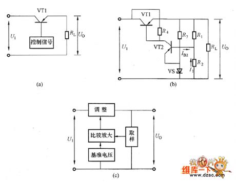
The transistors series voltage regulator circuit is shown in the picture. And, the picture (a) is equivalent circuit. The VT1 is adjustment transistor which is used to adjust the output voltage. The VT1 and load RL are in series. So this circuit is called the series voltage regulator circuit. Because the adjustment tube is using the transistors, the transistor series voltage regulator circuit could work under a big working current which could overcome the weakness that the zener diode regulator circuits output current is limited by the zener diode limiting current. The picture (b) is the practical series voltage regulator circuit. The picture (c) is its diagram circuit.
Continue Reading[...]

LM4651 and LM4652 170W power amplifier

170 Watt power amplifier is a power amplifier that is built by IC LM4651 and LM4652.

Part of this power amplifier driver using the LM4651 IC designed specifically for the purpose of the class AB amplifier driver with short circuit protection feature, containing under voltage, thermal shutdown protection and standby functions. Section 170 Watt power amplifier using LM4651 IC with a MOSFET power amplifier is equipped with temperature sensors that will be used by IC LM4651 as controlnya thermal signal. IC IC LM4651 and LM4652 are designed specifically to each other in pairs to create a class AB power amplifier with protection features are detailed. Detailed series of 170 Watt power amplifier can be seen in thethe following figure .

LM4651 and LM4652 170W power amplifier

Power amplifier circuit requires supply voltages +22 V DC symmetrical 0-22V. Power Amplifier with IC LM4651 and LM4652 are often used in portable HiFi systems such as powered speakers, power subwoofer and car audio power Booter. D1, D2, D3 and D4 in series 170 watt power amplifier with LM4651 and LM4652 is a 22V zener diode.
Continue Reading[...]

Tuesday, April 9, 2013

Subwoofer Wiring Diagrams Dual Voice Coilspeakers

Subwoofer Wiring on Subwoofer Wiring Diagram
Subwoofer Wiring Diagram.


Subwoofer Wiring on Car Audio Parallel Speaker Wiring Diagram
Car Audio Parallel Speaker Wiring Diagram.


Subwoofer Wiring on Subwoofer Wiring Diagrams Understand Ohms Law
Subwoofer Wiring Diagrams Understand Ohms Law.


Subwoofer Wiring on How To  Additional Subwoofer System Wiring Connection For Vw Golf Iv
How To Additional Subwoofer System Wiring Connection For Vw Golf Iv.


Subwoofer Wiring on Basic Subwoofer Wiring  For More Information  Check Out Our Subwoofer
Basic Subwoofer Wiring For More Information Check Out Our Subwoofer.


Subwoofer Wiring on Ideally The Power Capacitor Should Be As Close As Possible
Ideally The Power Capacitor Should Be As Close As Possible.


Subwoofer Wiring on Choosing Subwoofer Wiring For Your Passive And Powered Subwoofer Box
Choosing Subwoofer Wiring For Your Passive And Powered Subwoofer Box.


Subwoofer Wiring on Car Stereos  Amp And Subwoofer Wiring   4 Ohm Dvc Sub Or 2ohm Dvc Sub
Car Stereos Amp And Subwoofer Wiring 4 Ohm Dvc Sub Or 2ohm Dvc Sub.


Subwoofer Wiring on Wiring A Sub To Pre Existing Amp Speakers    Honda Tech
Wiring A Sub To Pre Existing Amp Speakers Honda Tech.


Subwoofer Wiring on Subwoofer Wiring Diagrams  Two 2 Ohm Dual Voice Coil  Dvc  Speakers
Subwoofer Wiring Diagrams Two 2 Ohm Dual Voice Coil Dvc Speakers.


Continue Reading[...]

Trailer Wiring Diagram Light Plug Brakes Hitch Wire Brake

Boat Trailer Wiring Diagram on Terminal Number Function 7 Core Wire Colour 1 Reversing Light Yellow 2
Terminal Number Function 7 Core Wire Colour 1 Reversing Light Yellow 2.


Boat Trailer Wiring Diagram on Trailer Wiring Diagram Light Plug Brakes Hitch 7 Pin Way Wire Brake
Trailer Wiring Diagram Light Plug Brakes Hitch 7 Pin Way Wire Brake.


Boat Trailer Wiring Diagram on All New Ck Trailer Tow Wiring Diagram Png
All New Ck Trailer Tow Wiring Diagram Png.


Boat Trailer Wiring Diagram on 2007 20ft Sea Ray 200 Sundeck Share This   25
2007 20ft Sea Ray 200 Sundeck Share This 25.


Boat Trailer Wiring Diagram on Http   Www Wiringdiagrams21 Com Wp C   Ng Diagram Png
Http Www Wiringdiagrams21 Com Wp C Ng Diagram Png.


Boat Trailer Wiring Diagram on Diagram Shows How The T Connector Works On Vehicles That
Diagram Shows How The T Connector Works On Vehicles That.


Boat Trailer Wiring Diagram on Example Wiring Diagram For Multiple Battery Cutoff Switches
Example Wiring Diagram For Multiple Battery Cutoff Switches.


Boat Trailer Wiring Diagram on Boat Trailer Fenders  1981 Fender Deluxe Reverb Amp Wiring Diagram
Boat Trailer Fenders 1981 Fender Deluxe Reverb Amp Wiring Diagram.


Boat Trailer Wiring Diagram on Sj23 Tech Tip A08   A Guide To Maintain Trailer Lights And Wiring
Sj23 Tech Tip A08 A Guide To Maintain Trailer Lights And Wiring.


Boat Trailer Wiring Diagram on Proper Trailer Wiring Determines The Tow Capabilities Of A Trailer
Proper Trailer Wiring Determines The Tow Capabilities Of A Trailer.


Continue Reading[...]

Build a Radio Wave Alarm

This simple circuit is sure to have the police beating a path to your door- however, it has the added advantage of alerting you to their presence even before their footsteps fall on the doormat.

Simple Radio Wave Alarm Circuit Diagram :
Build a Radio Wave Alarm

Notes :
  • The circuit transmits on Medium Wave (this is the small problem with the police). IC1a, together with a sensor (try a 20cm x 20cm sheet of tin foil) oscillates at just over 1MHz. This is modulated by an audio frequency (a continuous beep) produced by IC1b. When a hand or a foot approaches the sensor, the frequency of the transmitter (IC1a) drops appreciably.
  • Suppose now that the circuit transmits at 1MHz. Suppose also that your radio is tuned to a frequency just below this. The 1MHz transmission will therefore not be heard by the radio. But bring a hand or a foot near to the sensor, and the transmitters frequency will drop, and a beep will be heard from the radio.
  • Attach the antenna to a multiplug adapter that is plugged into the mains, and you will find that the Medium Wave transmission radiates from every wire in your house. Now place a suitably tuned Medium Wave radio near some wires or a plug point in your house, and an early-warning system is set up.
  • Instead of using the sheet of tin foil as the sensor, you could use a doorknob, or burglar bars. Or you could use a pushbutton and series resistor (wired in series with the 33K resistor - the pushbutton would short it out) to decrease the frequency of IC1a, so activating the system by means of a pushbutton switch. In this case, the radio would be tuned to a frequency just below that of the transmitter.
Continue Reading[...]

Loudspeaker Impedance Meter

Also suitable for Headphones Operates in conjunction with a DVM
A simple Impedance Meter can be useful to measure the actual impedance a loudspeaker or headphone is presenting @ 1kHz standard frequency. The circuit, designed on request, relies on an earlier design (Spot-frequency Sine wave Generator) to obtain a stable, low distortion 1kHz sine wave avoiding the use of thermistors, bulbs or any special amplitude-limiting device. The sine wave output, after some amplitude setting obtained by means of P1, is sent to the device under measurement through a resistor.

A regulated supply is necessary to obtain a stable output waveform. D1 and D2 force IC1 to deliver 6.2V output instead of the nominal 5V. The measurement is done in two stages: as a constant current supply of the device under test is necessary, this can be set at first by adjusting P1 and measured across the series resistor (R7 or R8, depending on the impedance value to be measured); then, the meter is switched across the device under test and the actual impedance will be read directly on the meter display.
Circuit diagram:
Loudspeaker Impedance Meter Circuit DaigramLoudspeaker Impedance Meter Circuit Diagram 
Parts:
P1_______________4K7  Linear Potentiometer
R1______________12K 1/4W Resistor
R2_______________2K2 1/4W Resistor
R3_______________1K 1/2W Trimmer (Cermet)
R4_______________1K5 1/4W Resistor
R5_______________4K7 1/4W Resistor
R6_______________3K3 1/4W Resistor
R7_____________100R 1/4W Resistor (See Notes)
R8_______________1K 1/4W Resistor (See Notes)
R9_______________1K 1/4W Resistor (Optional)
C1______________22nF 63V Polyester Capacitor
C2_____________330nF 63V Polyester Capacitor
C3______________22µF 25V Electrolytic Capacitor
D1,D2_________1N4148 75V 150mA Diodes
D3_______________3mm Red LED (Optional)
Q1,Q2,Q3_______BC550C 45V 100mA Low noise High gain NPN Transistors
IC1____________78L05 5V 100mA Regulator IC
SW1,SW2_________SPDT Toggle or Slider Switches
SW3_____________SPST Toggle or Slider Switch
B1________________9V PP3 Battery

Clip for PP3 Battery
Circuit set-up using an oscilloscope:

Connect the oscilloscope in place of the DVM and rotate P1 fully clockwise.
Short the speaker output and adjust R3 to obtain a sine wave of about 2.2V peak-to-peak amplitude.

"By ear" circuit set-up:

Connect a small loudspeaker or one of the two earpieces forming a pair of headphones to the circuit output and rotate P1 to obtain a moderate output sound level.

Carefully adjust R3 until the output sound will stop; then turn back the trimmer very slowly and stop adjusting immediately when the sound will start again.

Measurement:
  • Connect a Digital Voltage Meter set to 200mV ac range to the DVM output terminals
  • Connect the device under test to the Speaker terminals
  • Switch SW1 in the position towards R7 if the impedance value to be measured is below 100 Ohm or towards R8 if above
  • With SW2 in the "Set" position power-on the circuit by means of SW3
  • Adjust P1 in order to read exactly 100.0mV on the DVM display
  • Switch SW2 in the "Measure" position and read directly the loudspeaker or headphones impedance value on the DVM display, e.g. 8.5mV = 8.5 Ohm
  • Please note that when measuring devices with impedance values above 100 Ohm (SW1 set towards R8), the decimal point in the DVM reading must be ignored. E.g. if the display shows 70.5mV, the impedance will be 705 Ohm

Notes:
  • For very precise measurements use 1% or 2% tolerance resistors for R7 and R8.
  • D3 LED pilot light and its current limiting resistor R9 are optional.

Streampowers
Continue Reading[...]

Fuse Box Ford 1994 1998 Mustang Battery Junction Diagram

Fuse Box Ford 1994-1998 Mustang Battery Junction Diagram - Here are new post for Fuse Box Ford 1994-1998 Mustang Battery Junction Diagram.

Fuse Box Ford 1994-1998 Mustang Battery Junction Diagram


Fuse Box Ford 1994-1998 Mustang Battery Junction Diagram

Fuse Panel Layout Diagram Parts: constant control relay, main light switch, multifunction switch, starter motor relay, instrument cluster, ABS module, instrument panel, reversing lamp, speed control, daytime running light, ABS module, auxiliary power point, main light switch, rear window defrost, power door lock, CD player, horn, power seat switch, generator, constant control relay, intake manifold relay module.
Continue Reading[...]