Friday, December 27, 2013
Intelligent Electronic Lock

When four password digits in ‘0’ through ‘9’ are mixed with the remaining six digits connected across disable switch terminals, energisation of relay RL1 by unauthorised person is prevented. For authorized persons, a 4-digit password number is easy to remember. To energise relay RL1, one has to press switches S1 through S4 sequentially within six seconds, making sure that each of the switch is kept depressed for a duration of 0.75 second to 1.25 seconds.
The relay will not operate if ‘on’ time duration of each tactile switch (S1 through S4) is less than 0.75 second or more than 1.25 seconds. This would amount to rejection of the code. A special feature of this circuit is that pressing of any switch wired across disable switch (S6) will lead to disabling of the whole electronic lock circuit for about one minute. Even if one enters the correct 4-digit password number within one minute after a ‘disable’ operation, relay RL1 won’t get energized.
So if any unauthorized person keeps trying different permutations of numbers in quick successions for energization of relay RL1, he is not likely to succeed. To that extent, this electronic lock circuit is fool-proof. This electronic lock circuit comprises disabling, sequential switching, and relay latch-up sections. The disabling section comprises zener diode ZD5 and transistors T1 and T2. Its function is to cut off positive supply to sequential switching and relay latch-up sections for one minute when disable switch S6 (or any other switch shunted across its terminal) is momentarily pressed.
During idle state, capacitor C1 is in discharged condition and the voltage across it is less than 4.7 volts. Thus zener diode ZD5 and transistor T1 are in non-conduction state. As a result, the collector voltage of transistor T1 is sufficiently high to forward bias transistor T2. Consequently, +12V is extended to sequential switching and relay latch-up sections. When disable switch is momentarily depressed, capacitor C1 charges up through resistor R1 and the voltage available across C1 becomes greater than 4.7 volts.
Thus zener diode ZD5 and transistor T1 start conducting and the collector voltage of transistor T1 is pulled low. As a result, transistor T2 stops conducting and thus cuts off positive supply voltage to sequential switching and relay latch-up sections. Thereafter, capacitor C1 starts discharging slowly through zener diode D1 and transistor T1. It takes approximately one minute to discharge to a sufficiently low level to cut-off transistor T1, and switch on transistor T2, for resuming supply to sequential switching and relay latch-up sections; and until then the circuit does not accept any code.
The sequential switching section comprises transistors T3 through T5, zener diodes ZD1 through ZD3, tactile switches S1 through S4, and timing capacitors C2 through C4. In this three-stage electronic switch, the three transistors are connected in series to extend positive voltage available at the emitter of transistor T2 to the relay latch-up circuit for energising relay RL1. When tactile switches S1 through S3 are activated, timing capacitors C2, C3, and C4 are charged through resistors R3, R5, and R7, respectively.
Timing capacitor C2 is discharged through resistor R4, zener diode ZD1, and transistor T3; timing capacitor C3 through resistor R6, zener diode ZD2, and transistor T4; and timing capacitor C4 through zener diode ZD3 and transistor T5 only. The individual timing capacitors are chosen in such a way that the time taken to discharge capacitor C2 below 4.7 volts is 6 seconds, 3 seconds for C3, and 1.5 seconds for C4. Thus while activating tactile switches S1 through S3 sequentially, transistor T3 will be in conduction for 6 seconds, transistor T4 for 3 seconds, and transistor T5 for 1.5 seconds.
The positive voltage from the emitter of transistor T2 is extended to tactile switch S4 only for 1.5 seconds. Thus one has to activate S4 tactile switch within 1.5 seconds to energise relay RL1. The minimum time required to keep switch S4 depressed is around 1 second. For sequential switching transistors T3 through T5, the minimum time for which the corresponding switches (S1 through S3) are to be kept depressed is 0.75 seconds to 1.25 seconds.
If one operates these switches for less than 0.75 seconds, timing capacitors C2 through C4 may not get charged sufficiently. As a consequence, these capacitors will discharge earlier and any one of transistors T3 through T5 may fail to conduct before activating tactile switch S4. Thus sequential switching of the three transistors will not be achieved and hence it will not be possible to energise relay RL1 in such a situation. A similar situation arises if one keeps each of the mentioned tactile switches de-pressed for more than 1.5 seconds.
When the total time taken to activate switches S1 through S4 is greater than six seconds, transistor T3 stops conducting due to time lapse. Sequential switching is thus not achieved and it is not possible to energise relay RL1. The latch-up relay circuit is built around transistors T6 through T8, zener diode ZD4, and capacitor C5. In idle state, with relay RL1 in de-energised condition, capacitor C5 is in discharged condition and zener diode ZD4 and transistors T7, T8, and T6 in non-conduction state.
However, on correct operation of sequential switches S1 through S4, capacitor C5 is charged through resistor R9 and the voltage across it rises above 4.7 volts. Now zener diode ZD4 as well as transistors T7, T8, and T6 start conducting and relay RL1 is energised. Due to conduction of transistor T6, capacitor C5 remains in charged condition and the relay is in continuously energised condition. Now if you activate reset switch S5 momentarily, capacitor C5 is immediately discharged through resistor R8 and the voltage across it falls below 4.7 volts. Thus zener diode ZD4 and transistors T7, T8, and T6 stop conducting again and relay RL1 de-energises.
Wednesday, December 25, 2013
Simple Microprocessor power supply watchdog circuit Diagram

Monday, December 23, 2013
Build a Remotely Adjustable Solid State High voltage Supply Circuit Diagram

Saturday, December 21, 2013
Battery Powered High voltage Generator Circuit Diagram

Thursday, December 19, 2013
Video Tracer Circuit Diagram
Video Tracer Circuit diagram:

Tuesday, December 17, 2013
ANTI BAG SNATCHING ALARM
 |
| www.blogger.com |
Tuesday, October 8, 2013
Low Battery Indicator I

Sunday, October 6, 2013
FLASH LIGHT ELECTRONIC DIAGRAM

IC NE555 works as an astable multivibrator with variation on the frequency. With this circuit, the LED blinks every half second. How long the blink time is, can be adjusted by adjusting the value of capacitor C1. Up to 18 additional LEDs can be attached to this circuit (36 LEDs total).
Components :
Diode D1-D2 : 5mm LED
Resistor R1 : 4K7 ohm
Resistor R2 : 1k ohm
Resistor R3-R4 : 330 ohm
Variable resistor VR1 : 100k ohm
Polar capacitor C1 : 10 uF/10 V
Capacitor C2 : 0.01 uF
IC1 : NE555
6V power supply
Friday, October 4, 2013
RIAA Phono Preamplifier
In that simple design, the first 741 simply amplified the full range of the frequency spectrum, while the second one was fitted with RIAA frequency compensation — a fairly common configuration at that time. However, a variant on this classic design was recently born after a bit of experimenting. It also uses two opamps, with the difference that the RIAA frequency compensation is distributed over both opamps. The accompanying figure shows the schematic diagram of this preamplifier. The first opamp attenuates the signal at 6 dB/octave starting at 2.2 kHz, while the second opamp looks after the other corner frequency.

The objective of the new design was to keep the feedback factor as high as possible in both stages. To the considerable surprise of the developer, this modification turned out to have an unexpected side effect: when records were played, certain scratches were no longer audible! The difference between the new and old preamplifiers could be clearly heard; it was certainly not just imagination. What could be the cause of this? A quick calculation showed that a 0.05-mm scratch in a record groove moving past a needle at a speed of 0.5 m/s produces a square-wave pulse with a frequency of 10 kHz. Evidently, there is a lot to be gained by attenuating such pulses with a low-pass filter as early as possible, which means in the first stage, in order to prevent them from over-driving the rest of the circuit.
Wednesday, October 2, 2013
2 Line Intercom Cum Telephone Line Changeover Circuit
As a result, buzzer PZ2 sounds. Simultaneously, the side tone is heard in the speaker of handset of phone 1. The person at phone 2 could then lift the handset and start conversation. Similar procedure is to be followed for initiation of the conversation from phone 2 using switch S2. In this mode of operation, a 3-pole, 2-way slide-switch S3 is to be used as shown in the figure. In the changeover mode of operation, switch S3 is used to changeover the telephone line for use by telephone 2. The switch is normally in the intercom mode and telephone 3 is connected to the exchange line. Before changing over the exchange line to telephone 2, the person at telephone 1 may inform the person at telephone 2 (in the intercom mode) that he is going to changeover the line for use by him (the person at telephone 2).
 As soon as changeover switch S3 is flipped to the other position, 12V supply is cut off and telephones 1 and 3 do not get any voltage or ring via the ring-tone-sensing unit. Once switch S3 is flipped over for use of exchange line by the person at telephone 2, and the same (switch S3) is not flipped back to normal position after a telephone call is over, the next telephone call via exchange lines will go to telephone 2 only and the ringtone-sensing circuit will still work. This enables the person at phone 3 to know that a call has gone through. If the handset of telephone 3 is lifted, it is found to be dead. To make telephone 3 again active, switch S3 should be changed over to its normal position.
Saturday, September 28, 2013
9V HEADPHONE AMPLIFIER NE5534 ELECTRONIC DIAGRAM

I have Used it with Sennheiser 465s and achieved ear-splitting volume. The amplifier is ideal as a booster for power-conserving stereo sources Such as portable CD players and for interfacing with passive EQ networks Such as tone controls or a headphone acoustic simulator.
Thursday, September 26, 2013
Discrete Voltage Regulator
 They are to be found in three areas: voltage range, bandwidth and current rating. The last of these is the primary strength of this circuit, since the maximum current depends only on the specifications of the output transistor. With the BD680, as used here, a current of 4 A can be delivered at a collect-emitter voltage of 10 V with adequate cooling (Rth = 3.12 K/W). The peak current is even 6 A. Try matching that with an integrated voltage regulator! The maximum input voltage is 30 V with the illustrated version of the circuit (UDSmax of T1), but this can easily be increased by using special high-voltage transistors.
 The same applies to the bandwidth, which can be extended as desired, without any modifications to the circuit, by using high-speed transistors. Generally speaking, wide bandwidth is also not one of the strong points of integrated voltage regulators. As noted, the circuit is basically very simple. A zener diode (D1) fed with a constant current of around 1mA by a JFET current source (T1) provides the reference potential. C1 is connected in parallel with D1 to provide well-behaved startup behaviour (soft start). This capacitor also provides additional buffering and decouples noise and other disturbances. The startup time is around three seconds.
The only additional item that is needed for the voltage regulator is an output buffer for the reference potential. This takes the form of a sort of super-Darlington using T2 and T3. This works very well, but has the disadvantage that the output voltage is a bit lower (one diode drop) than the Zener voltage. P1 can be added to correct this, but this does reduce the regulation of the circuit. If the voltage difference is not important, it is thus better to replace P1 with a wire jumper. The main specifications of the voltage regulator are listed in Table 1.
Tuesday, September 24, 2013
Luxury Car Interior Light
 Two opamps are generally required to generate a good triangle wave, but because the waveform doesn’t have to be accurate, we can make do with a single opamp. This results in the circuit around IC1.A, a relaxation oscillator supplying a square wave output. The voltage at the inverting input has more of a triangular shape. This signal can be used as long as we do not put too much of a load on it. The high impedance input of IC1.B certainly won’t cause problems in this respect. This opamp is used as a comparator and compares the voltage of the triangular wave with that across the door switch. When the door is open, the switch closes and creates a short to the chassis of the car.
 The output of the opamp will then be high, causing T1 to conduct and the interior light will turn on. When the door is closed the light will continue to burn at full strength until the voltage across C2 reaches the lower side of the triangle wave (about 5 V). The comparator will now switch its output at the same rate of the triangle wave (about 500 Hz), with a slowly reducing pulse width, which results in a slowly reducing brightness of the interior light. R8 and C3 protect the circuit from voltage spikes that may be induced by the fast switching of the light. The delay and dimming time can be adjusted with R6 and C2. Smaller values result in shorter times. You can vary the dimming time on its own by adjusting R1, as this changes the amplitude of the triangle wave across C1.
 R7 limits the discharge current of C2; if this were too big,it would considerably reduce the lifespan of the capacitor. There is no need to worry about reducing the life of the car battery. The circuit consumes just 350 µA when the lamp is off and a TLC272 is used for the dual opamp. A TL082 will take about 1 mA. These values won’t discharge a normal car battery very quickly; the self-discharge is probably many times higher. It is also possible to use an LM358, TL072 or TL062 for IC1. R8 then needs to have a value between 47 Ω and 100 Ω. Since T1 is always either fully on or fully off, hardly any heat is generated.
At a current of 2 A the voltage drop across the transistor is about 100 mV, giving rise to a dissipation of 200 mW. This is such a small amount that no heatsink is required. The whole circuit can therefore remain very compact and should be easily fitted in the car, behind the fabric of the roof for example.
Resistors:
R1,R2,R6 = 120kΩ
R3,R4 = 100kΩ
R5 = 470Ω
R7 = 100Ω
R8 = 220Ω
Capacitors:
C1 = 10nF
C2 = 100µF-25V
C3 = 10µF-25V
Semiconductors:
T1 = BUZ10
IC1 = TLC272CP
Sunday, September 22, 2013
DC Control for Triacs
 This has the advantage of generating less interference compared to switching the triac at arbitrary phase in a cycle. Indeed, it means that we can dispense with the suppressor choke at the output that would otherwise be necessary. If very brief pulses are likely to be present at the input to the opto-coupler, a 220 nF capacitor should be connected between the input of the circuit and the emitter of T1 to lengthen the drive pulses. This ensures that the triac will be triggered even with very short input pulses, which might otherwise miss the zero-crossing point of the mains waveform. The triac should be an AW-suffix type. These types are less sensitive, but have higher dv/dt and di/dt specifications. The gate resistance must be constructed from two resistors connected in series, since normal resistors are not suitable for direct use with mains voltages. It is also necessary to exercise care around the opto-coupler. In order to guarantee Class II isolation the solder pads on the input and output sides must be separated by at least 6 mm. The leads may therefore need to be bent outwards when soldering.
Friday, September 20, 2013
1997 Chevrolet Blazer Electrical Wiring Diagram
 |
| 1997 Chevrolet Blazer Electrical Wiring Diagram |
Thursday, September 12, 2013
Simple FM Transmitter Circuit Diagram

Tuesday, September 10, 2013
Touch Controlled Mute Switch Circuit Diagram
Touch controlled Mute switch circuit diagram

Wednesday, September 4, 2013
Dual Level Liquid Sensor
Dual Level Liquid Sensor Circuit Diagram

Monday, September 2, 2013
2 Cell Lithium Ion Charger
When the battery is low, the current pulses are spaced close together so that a somewhat constant current is present. As the batteries reach full charge, the pulses are spaced farther apart and the full charge condition is indicated by the LED blinking at a slower rate. A TL431, band gap voltage reference (2.5 volts) is used on pin 6 of the comparator so the comparator output will switch low, triggering the 555 timer when the voltage at pin 7 is less than 2.5 volts.
The 555 output turns on the 2 transistors and the batteries charge for about 30 milliseconds. When the charge pulse ends, the battery voltage is measured and divided down by the combination 20K, 8.2K and 620 ohm resistors so when the battery voltage reaches 8.2 volts, the input at pin 7 of the comparator will rise slightly above 2.5 volts and the circuit will stop charging.
2 Cell Lithium Ion Charger Circuit diagram

The circuit could be used to charge other types of batteries such as Ni-Cad, NiMh or lead acid, but the shut-off voltage will need to be adjusted by changing the 8.2K and 620 ohm resistors so that the input to the comparator remains at 2.5 volts when the terminal battery voltage is reached. For example, to charge a 6 volt lead acid battery to a limit of 7 volts, the current through the 20K resistor will be (7-2.5)/ 20K = 225 microamps. This means the combination of the other 2 resistors (8.2K and 620) must be R=E/I = 2.5/ 225 uA = 11,111 ohms. But this is not a standard value, so you could use a 10K in series with a 1.1K, or some other values that total 11.11K
Be careful not to overcharge the batteries. I would recommend using a large capacitor in place of the battery to test the circuit and verify it shuts off at the correct voltage.
Saturday, August 31, 2013
Simple Field Strength Meter
Simple Field Strength Meter Circuit diagram:

Parts List:
1 OA91 Germanium Diode
1 3.3M Resistor
1 100p Capacitor
L1 7 turns on a 1/4 inch former (suitable for around 100MHz)
Notes:
The multimeter should be set to the lowest dc volts range for maximum sensitivity. This is normally 200mV DC for most meters. The circuit works well at VHF (around 100MHz) and was quite pleased with the results. L1 was 7 turns on a quarter inch former with ferrite slug. This covered the UK FM band.
A digital multimeter, as opposed to an analogue signal meter offers several advantages in this circuit. First, the impedance of a digital meter is very high, around 10Meg/Volt on most meters. This does not shunt the tank circuit unduly. Second, compared to an analogue meter, very slight differences in signal strength can be more easily observed. Thirdly,a digital meter will have better linearity, responding well to both weak and stronger signals.
Thursday, August 15, 2013
Active band reject filter Circuit

Tuesday, August 13, 2013
TV Protect Circuit Dead or Damaged
 |
| Protect IC |
- Protectors x-ray
- Vertical Protectors
- Protectors B + over current (OCP)
- Protectors B + over voltage (OVP)
- ABL Protectors
- Supply voltage surge protector (if short or broken)
- Protectors white balance
- Protectors circuit power supply (SMPS)
Sunday, August 11, 2013
Simple Output limiter Circuit Diagram
Simple Output-limiter Circuit Diagram

Friday, August 9, 2013
Mobile Phone and iPod Battery Charger
Charge your iPod without connecting it to a computer!
Using the USB port on your computer to charge your player’s batteries is not always practical. What if you do not have a computer available at the time or if you do not want to power up a computer just for charging? Or what if you are traveling? Chargers for Mobile Phones iPods and MP3 players are available but they are expensive and you need separate models for charging at home and in the car.
This charger can be used virtually anywhere. While we call the unit a charger, it really is nothing more than a 5V supply that has a USB outlet. The actual charging circuit is incorporated within the iPOD or MP3 player itself, which only requires a 5V supply. As well as charging, this supply can run USB-powered accessories such as reading lights, fans and chargers, particularly for mobile phones.
The supply is housed in a small plastic case with a DC input socket at one end and a USB type "A" outlet at the other end, for connecting to Mobile Phone, an iPod or MP3 player when charging. A LED shows when power is available at the USB socket. Maximum current output is 660mA, more than adequate to run any USB-powered accessory.
Pictures, PCB and Circuit Diagram:
 Front View Of Mobile Phone and iPod Battery Charger Circuit
 Bottom View Of Mobile Phone and iPod Battery Charger Circuit
 PCB Layout Of Mobile Phone and iPod Battery Charger Circuit
 Mobile Phone and iPod Battery Charger Circuit Diagram
| Parts | Description |
| P1 | 1K |
| R1 | 1R-0.5W |
| R2 | 1R-0.5W |
| R3 | 1R-0.5W |
| R4 | 1K |
| R5 | 560R |
| R6 | 10R-0.5W |
| R7 | 470R |
| C1 | 470uF-25V |
| C2 | 100nF-63V |
| C3 | 470pF |
| C4 | 100uF-25V |
| D1 | 1N5404 |
| D2 | 1N4001 |
| D3 | 1N5819 |
| D4 | 5.1V-1W Zener Diode |
| D5 | 5mm. Red LED |
| L1 | 220uH |
| S1 | USB A Type Socket |
| SW1 | On/Off Switch |
| IC1 | MC34063A |
Specifications:
Output voltage ----------------------5V
Output current ---------------------660mA maximum for 5V out
Input voltage range ------------------9.5V to 15V DC
Input current requirement ----------500mA for 9V in, 350mA for >12V input
Input current with output shorted--- 120mA at 9V in, 80mA at 15V in
Output ripple ------------------------14mV (from no load to 660mA)
Load regulation ----------------------25mV (from no load to 660mA)
Line regulation ----------------------20mV change at full load from 9 to 18V input
No load input current ----------------20mA
(The specification for the computer USB 2.0 port requires the USB port to deliver up to 500mA at an output voltage between 5.25V and 4.375V).
The circuit is based around an MC34063 switch mode regulator. This has high efficiency so that there is very little heat produced inside the box, even when delivering its maximum output current. The circuit is more complicated than if we used a 7805 3-terminal regulator but since the input voltage could be 15V DC or more, the voltage dissipation in such a regulator could be 5W or more at 500mA. and 5W is far too much for a 7805, even with quite a large heatsink. Credit for this circuit goes to SiliconChip, A wonderful electronics magazine.
Source :www.extremecircuits.net
Wednesday, August 7, 2013
50W Offline Switching Power supply Circuit Diagram

Monday, August 5, 2013
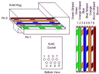
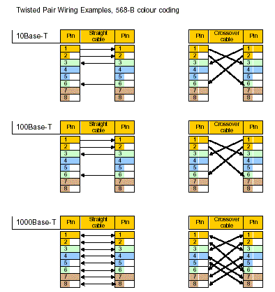
Wiring Diagram

Network Cable Use Either 568a Or Most Common 568b Wiring On Both Ends.
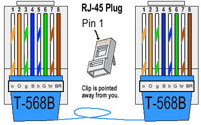
How To Make A Cat5e Network Cable Miscellaneous Items.
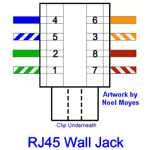
Diagram Of Correct Color Alignment For Making Cat5e Network Wall Jack.
Mica Machine Information Consulting Alliance Windows Xp Help.

Cross Over Cable Just Uses The Wiring Configuration From Each.

How To Wire A Cat5 Eia 568 A Cable.

78 Responses To How To Install An Ethernet Jack For A Home Network.

Fs Asus P8p67 Motherboard And Amd Xfx 6950.

Cat 5e Wiring Diagram.
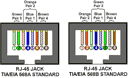
Cat5e Cable Cat 5e Cables Patch Cords.
Saturday, August 3, 2013
Cat7 Cables Unshielded Twisted Pairethernet Wiring

Crossover Ethernet Cable.

Figure 3 Tie Eia T568 Ethernet Wiring Standards.

Cat7 Cables 100 Ohm Utp Unshielded Twisted Pair Ethernet Wiring.

Switched Ethernet Modern Ethernet Implementations Often Look Nothing.

Figure 4 Wiring Diagram For An Ethernet Crossover Cable.
Detailed Graph For Coloring Scheme Eia 568 Is.
Diagram Of Correct Color Alignment For Making Cat5e Network Cable.
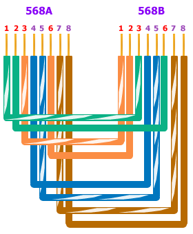
Category 5 Wiring Scheme Straight Through Cable Vs Crossover Cable.

Do It Yourself Roll Your Own Network Cables.
Beginnercode Com Connecting Network Cable Ends.