Showing posts with label diagram. Show all posts
Showing posts with label diagram. Show all posts
Wednesday, December 25, 2013
Simple Microprocessor power supply watchdog circuit Diagram
The Simple Microprocessor power supply watchdog circuit Diagram monitors the input to the microprocessor 5 V regulated supply for voltage drops and initiates a reset sequence before supply regulation is lost. In operation, the resistor capacitor combination Rs and Cj form a short time constant smoothing network for the output of the fullwave bridge rectifier.
An approximately triangular, voltage waveform appears across C and Rs and it is the minimum excursion of this that initiates the reset. Diode Dg prevents charge sharing between capacitors Cj and Ck. Resistors Rn and Rm form a feedback network around the voltage reference section of the LM10C, setting a threshold voltage of 3.4 volts.
Microprocessor power supply watchdog circuit Diagram

The threshold voltage is set at 90% of the minimum voltage of the triangular waveform. When the triangular wave trough, at the comparators non-inverting input, dips below the threshold, the comparator output is driven low. This presents a reset to the microprocessor. Capacitor Ch is charged slowly through resistor Rk and discharged rapidly through diode De.
Monday, December 23, 2013
Build a Remotely Adjustable Solid State High voltage Supply Circuit Diagram
How to build a remotely adjustable solid state high-voltage supply Circuit Diagram. The output voltage changes approximately linearly up to 20 KV as the input voltage is varied from 0 to 5 V. The oscillator is tuned by a 5-0 potentiometer to peak the output voltage at the frequency of maximum transformer response between 45 and 55 kHz.
The feedback voltage is applied through a 100-KO resistor, an op amp, and a comparator to a high-voltage amplifier. A diode and varistors on the primary side of the transformer protect the output transistor. The transformer is a flyback-type used in color-television sets. A feedback loop balances between the high-voltage output and the low-voltage input.
Remotely Adjustable Solid State High-voltage Supply Circuit Diagram

Remotely Adjustable Solid State High-voltage Supply Circuit Diagram
Saturday, December 21, 2013
Battery Powered High voltage Generator Circuit Diagram
This is the battery powered high-voltage generator circuit diagram. Output voltage great enough to jump a l-inch gap can be obtained from a 12-V power source. A 555 timer IC is connected as an stable multi vibrator that produces a narrow negative pulse at pin 3. The pulse turns Ql on for the duration of the time period. The collector of Ql is direct-coupled to tbe base of tbe power transistor Q2, turning it on during the same time period.
The emitter of Q2 is direct -coupled through current limiting resistor R5 to the base of the power transistor. Q3 switches on, producing a minimum resistance between the collector and emitter. The high-current pulse going through tbe primary of high-voltage transformer Tl generates a very high pulse voltage at its secondary output terminal (labeled X). The pulse frequency is determined by tbe values of Rl, R2, and C2. The values given in the parts list were chosen to give the best possible performance when an auto-ignition coil is used for Tl.
Battery Powered High-voltage Generator Circuit Diagram

Thursday, December 19, 2013
Video Tracer Circuit Diagram
This circuit was designed as an aid to installers and maintainers of video systems. It is basically a video sync separator (IC1) followed by a LED and buzzer driver (IC2, Q1 & Q2). In use, the device is connected to a video cable and if there is video present, the LED will flash at about 10Hz. If there is no video, the LED flashes briefly every couple of seconds. A buzzer can also be switched in to provide an audible indication. The buzzer is particularly useful when tracing cabling faults or trying to find a correct cable amongst many, where it is difficult to keep an eye on the LED.
Another use for the buzzer option is to provide a video fault indication. For example, it could be inserted in bridging mode, with switch S1 in high impedance mode (position 2) across a video line and set to alarm when there is no video present. If someone pulls out a cable or the video source is powered off, the alarm would sound. IC1 is a standard LM1881 video sync separator circuit and 75Ω termination can be switched in or out with switch S1a. The other pole of the switch, S1b, turns on the power. The composite sync output at pin 1 is low with no video input and it pulses high when composite sync is detected.
Video Tracer Circuit diagram:

These pulses charge a 100nF capacitor via diode D1. When there is no video at the input, oscillator IC2b is enabled and provides a short pulse every couple of seconds to flash the LED. The duty cycle is altered by including D2, so that the discharge time for the 10μF capacitor is much shorter than the charge time. The short LED pulse is used as a power-on indicator drawing minimal average current. When video is present at the input, IC2b is disabled and IC2d is enabled. The output of IC2d provides a 10Hz square wave signal to flash the LED. The buzzer is controlled by switch S2. In position 2 the buzzer will sound when there is video at the input and in position 1 the buzzer will sound when there is no video at the input.
Source : http://www.ecircuitslab.com/2011/07/video-tracer-circuit-diagram.html
Sunday, October 6, 2013
FLASH LIGHT ELECTRONIC DIAGRAM

FLASH LIGHT ELECTRONIC DIAGRAM
IC NE555 works as an astable multivibrator with variation on the frequency. With this circuit, the LED blinks every half second. How long the blink time is, can be adjusted by adjusting the value of capacitor C1. Up to 18 additional LEDs can be attached to this circuit (36 LEDs total).
Components :
Diode D1-D2 : 5mm LED
Resistor R1 : 4K7 ohm
Resistor R2 : 1k ohm
Resistor R3-R4 : 330 ohm
Variable resistor VR1 : 100k ohm
Polar capacitor C1 : 10 uF/10 V
Capacitor C2 : 0.01 uF
IC1 : NE555
6V power supply
Saturday, September 28, 2013
9V HEADPHONE AMPLIFIER NE5534 ELECTRONIC DIAGRAM

9V HEADPHONE AMPLIFIER NE5534 ELECTRONIC DIAGRAM
I have Used it with Sennheiser 465s and achieved ear-splitting volume. The amplifier is ideal as a booster for power-conserving stereo sources Such as portable CD players and for interfacing with passive EQ networks Such as tone controls or a headphone acoustic simulator.
Friday, September 20, 2013
1997 Chevrolet Blazer Electrical Wiring Diagram
 |
| 1997 Chevrolet Blazer Electrical Wiring Diagram |
The Part of 1997 Chevrolet Blazer Electrical Wiring Diagram: Cruise Control System, Defogger, Rear
Glass Release, Rear Wiper/Washer, Shift Interlock System, Transmission System, 6-Way Power Seat Circuit, A/C Circuit, etc. Computer Data Lines, Anti-lock Brake, Back-up Lamps Circuit, Charging Circuit, Keyless Entry, Engine Performance Circuits, Warning System, Courtesy Lamps, Door Lock Circuit, Electronic Transfer Case Circuit, Exterior Lamps, Front Wiper/Washer, Starting Schematics, Supplemental Restraint, Sealed Beam Headlamps, Horn, Instrument Cluster Circuit, Instrument Illumination, Power Distribution Circuit, Headlight, Ground Distribution, Power Mirror, Power Window, Power Window Diagram, Features: Power windows, power door locks, anti-lock braking, dual air bag, power mirrors, cruise control, air conditioner, AM-FM stereo radio with CD, 4.3-liter Vortec V-6 engine, four-speed automatic gearbox.Thursday, September 12, 2013
Simple FM Transmitter Circuit Diagram
This circuit is a simple two transistor (2N2222) FM transmitter. No license is required for this transmitter according to FCC regulations regarding wireless microphones. If powered by a 9 volt battery and used with an antenna no longer than 12 inches, the transmitter will be within the FCC limits.
The microphone is amplified by Q1. Q2, C5, and L1 form an oscillator that operates in the 80 to 130 MHz range. The oscillator is voltage controlled, so it is modulated by the audio signal that is applied to the base of Q2. R6 limits the input to the RF section, and its value can be adjusted as necessary to limit the volume of the input. L1 and C6 can be made with wire and a pencil. The inductor (L1) is made by winding two pieces of 24 gauge insulated wire, laid side by side, around a pencil six times. Remove the coil you have formed and unscrew the two coils apart from each other.
FM Transmitter Circuit Diagram

One of these coils (the better looking of the two) will be used in the tank circuit, and the other can be used in the next one you build. The antenna (24 gauge wire) should be soldered to the coil you made, about 2 turns up from the bottom, on the transistor side, and should be 8-12 inches long. To make C6, take a 4 inch piece of 24 gauge insulated wire, bend it over double and, beginning 1/2" from the open end, twist the wire as if you were forming a rope. When you have about 1" of twisted wire, stop and cut the looped end off, leaving about 1/2" of twisted wire (this forms the capacitor) and 1/2" of untwisted wire for leads.
Tuesday, September 10, 2013
Touch Controlled Mute Switch Circuit Diagram
Here is another simple circuit to mute the volume of Audio devices through simple touch. It exploits the action of the flip-flops in the timer IC 555 to reduce the volume of the Audio amplifier. IC NE555 is designed in the toggle mode. Its lower and upper comparator inputs are connected to the touch plates which can be membrane switches or two pieces of conducting plates. The inputs of comparators are stabilized through R1 and R2 to avoid floating.
Touch controlled Mute switch circuit diagram

When the touch plate connected to pin 2 is touched momentarily, output of IC1 goes high and T1 conducts. The centre tap of the volume control is connected to the collector of T1. So when T1 conducts current going to the amplifier drains through T1. This reduces the volume.IC1 remains latched in this position with LED on. When the touch plate connected to pin 6 is touched momentarily, output of IC1 goes low and T1 turns off. This restores the volume.
Sunday, August 11, 2013
Simple Output limiter Circuit Diagram
Simple Output-limiter Circuit Diagram HA-5190 is rated for ±5 V output swing, and saturates at ±7 V. As with most op amps, recovery from output saturation is slow compared to the amplifier`s normal response time. Some form of limiting, either of the input signal or in the feedback path, is desirable if saturation might occur. The circuit illustrates a feedback limiter, where gain is reduced ifthe output exceeds ± ( Vz + 21j-). A 5-V zener with a sharp knee characteristic is recommended.
Simple Output-limiter Circuit Diagram

Wednesday, August 7, 2013
50W Offline Switching Power supply Circuit Diagram
The schematic shows a 50W power supply with a 5-V 10-A output. It is a fly back converter operating in the continuous mode. The circuit features a primary side and secondary side controller will full-protection from fault conditions such as over current. After the fault condition has been removed, the power supply will enter the soft-start cycle before recommencing normal operation.
50W Offline Switching Power supply Circuit Diagram

Monday, August 5, 2013
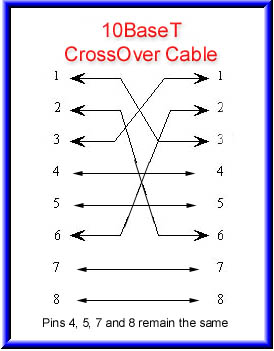
Wiring Diagram

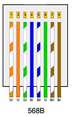
Network Cable Use Either 568a Or Most Common 568b Wiring On Both Ends.
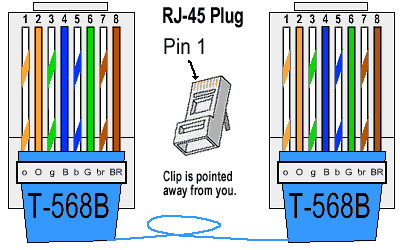
How To Make A Cat5e Network Cable Miscellaneous Items.
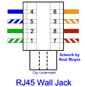
Diagram Of Correct Color Alignment For Making Cat5e Network Wall Jack.
Mica Machine Information Consulting Alliance Windows Xp Help.

Cross Over Cable Just Uses The Wiring Configuration From Each.

How To Wire A Cat5 Eia 568 A Cable.

78 Responses To How To Install An Ethernet Jack For A Home Network.

Fs Asus P8p67 Motherboard And Amd Xfx 6950.

Cat 5e Wiring Diagram.
Cat5e Cable Cat 5e Cables Patch Cords.
Tuesday, July 30, 2013
Tunable Bandpass Filter Circuit Diagram
One of the difficulties in the design of higher-order tunable bandpass filters is achieving correct tracking of the variable resistors in the RC networks. The use of switched capacitor networks can obviate that difficulty, as is shown in this filter. The filter can be divided roughly into two stages: an oscillator that controls the electronic switches arid the four phase-shift networks that provide the filtering proper.
Tunable Bandpass Filter Circuit Diagram

The oscillator, based on a 555, generates a pulsating signal whose frequency is adjustable over a wide range: the duty factor varies from 1:10 to 100:1. Electronic switches ESI through ES4 form the variable resistors whose value is dependent on the frequency of the digital signal. The operation of these switches is fairly simple. When they are closed, their resistance is about 60 ; when they are open, it is virtually infinitely high. a switch is closed for, say, 25% of the time, its average resistance is therefore 240 . `Varying the open:closed ratio of each switch varies the equivalent average resistance.
The switching rate of the switches must be much greater than the highest audio frequency to prevent audible interference between the audio and the clock signals. The input signal causes a given direct voltage across CI, so the op amp can be operated in a quasisym-metric manner, in spite of the single supply voltage. The direct voltage is removed from the output signal by capacitor C10. The fourth-order filter in the diagram can be used over the entire audio range and it has an amplification of about 40, although this depends to some extent on the clock frequency. The bandwidth depends mainly on the set frequency. The circuit draws a current of not more than 15 mA.
Sunday, July 28, 2013

Wednesday, June 5, 2013
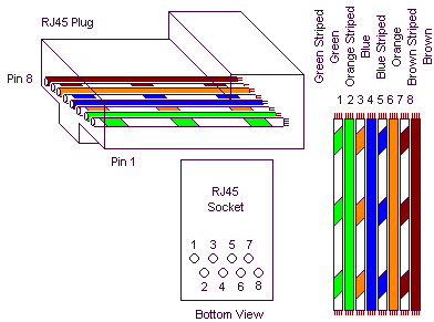
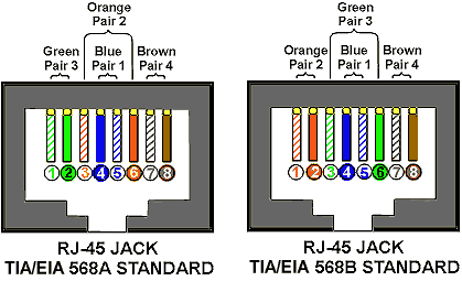
Rj45 Wiring Diagram
Cross Over Cable.

The Net Gate Rj 45 Cable Lay Out.

Rj45 Wiring Diagram.

Aui Cable Table A 2 Aui Cable Pin Outs Transceiver.

Rj45 How To Make A Network Cable.

Rj45 Wiring T568a Standard.
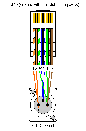
An Xlr To Rj45 Adaptor Will Allow The Use Of Cat5 Cable For.
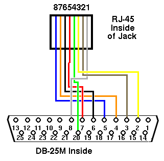
Serial To Rj 45 Adapters.

Serial Connection Db9 To Rj45.
Que Es Y Como Armar Un Rj45 Topologia Y Componented De Una Taringa.
Auto Electrical Wiring Diagram Manualcircuit Schematic
Royalty Free Stock Photography Electrical Wires Image 8885437.

Electrical Wire.

Auto Electrical Wiring Diagram Manual Circuit Schematic.

1966 Vw Beetle 1300 Electrical Wiring Diagram Jpg.

Carondelet Orthopaedic Surgeons Kansas City Howrah Bridge Songs Free.

Electrical Wiring Let S Talk Basic Residential Wiring.

Electrical Power Switchboard Stock Photo Download Professional.

Denver Co Home Electrical Wiring Electrical Contractors.

Wiring Circuits Wiring A Kitchen Electrical Circuits Needed When.

Find The 1995 Bmw 740il Series Electrical Wiring Diagram Here Pass.
Pontiac Fiero Headrest Speakers Wiring Diagram Wiring

From Articletrader Car Audio Wiring Diagram On Careleasedate Com.

This Wiring Diagram And Electrical System Apply For 1996 Nissan 300zx.

Anti Theft System And Alarm Circuit Wiring Diagram Circuit Schematic.

2003 Chevrolet Silverado C1500 Car Radio Wiring Diagram.

Details Of 2002 Honda Civic Immobilizer System Circuit Diagram.

Citroen Xantia Wiring Diagram And Body Electrical System Schematics.

Pontiac Fiero Headrest Speakers Wiring Diagram There Are Two Wiring.

Find More Info About 1996 Yamaha Tdm850 Wiring Diagram And.

Car Combination Flasher Typical Circuit Diagram Circuit Schematic.

Related Topics Car Audio Wiring Diagrams Car Stereo Wiring Diagram.
Subscribe to:
Posts (Atom)