Sunday, March 31, 2013

FM Wireless Microphone

Here
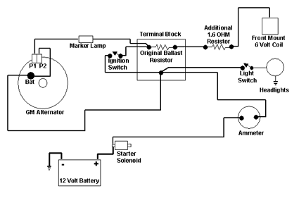
is a very simple, inexpensive and interesting project which provides
lot of fun to a home experimenter or hobbyist. This simple transmitter
can transmit speech over a short range. It can be used as a simple
cordless microphone. The circuit uses two integrated circuits from
Maxim. IC1 a MAX4467, is an amplifier raising the microphone signal to
a level suitable for frequency modulation (FM). IC2 is a
voltage-controlled oscillator (VCO) with integrated varactor (a.k.a.
varicap diode). Its nominal frequency of oscillation is set by inductor
L1. The inductor value 390 nH provides an oscillation frequency of
about 100 MHz. For best performance, L1 should be a high-Q component.
L1 may consist of 4 turns of silver-plated wire wound around a 10-mm
drill bit, and stretched to a length of about 1.5 cm.

The wire
diameter can be anything between 26 SWG (0.5 mm) and 20 SWG (1 mm). No
core is used. The MAX4467 is a micro-power opamp for low voltage
operation and providing 200-kHz gain bandwidth at a supply current of
just 24 µA. When used with an electret microphone, some form of DC bias
for the microphone capsule is necessary. The MAX4467 has the ability
to turn off the bias to the microphone when the device is in shutdown
mode. This can save several hundred micro-amps of supply current, which
can be significant in low power applications particularly for battery
powered applications like cordless microphones. The MIC-Bias pin
provides a switched version of Vcc to the bias components.

FM Wireless Microphone Circuit Diagram
Resistor
R1 resistor limits the current to the microphone element. The output
impedance of the MAX4467 is low and well suited to driving cables over
distances up to 50 m. The MAX2606 intermediate-frequency (IF)
voltage-controlled oscillators (VCO) has been designed specifically for
portable wireless communication systems. The IC comes in a tiny 6-pin
SOT23 package. The low-noise VCO features an on-chip varactor and
feedback capacitors that eliminate the need for external tuning
elements. Only an external inductor (here, L1) is required to set the
oscillation frequency and produce a properly operating VCO. To minimize
the effects of parasitic elements, which degrade circuit performance,
place L1 and C5 close to their respective pins.

Specifically,
place C5 directly across pins 2 (GND) and 3 (TUNE). Potentiometer P2
then lets you select a free channel by tuning over the FM band of 88 MHz
to 108 MHz. Output power is about –21dBm (approx. 10µW) into 50 Ω. P1
serves as a volume control by modulating the RF frequency. Signals
above 60mV introduce distortion, so the pot attenuates from that level.
To decrease stray capacitance, minimize trace lengths by placing
external components close to IC1’s pins. Using a wire antenna of about
75 cm the transmitter should have a range of about 35 m. Try to keep
all leads as short as possible to prevent stray capacitance. The
transmitter operates on a single supply voltage in the range 4.5 V to
5.5 V from any standard battery source. The transmitter must be housed
in a metal case, with shielding installed between the two stages (AF
and RF). Try to keep all leads as short as possible to prevent stray
capacitance.
Continue Reading[...]

Rear Light After Glow For Bicycles

This article is of interest only to readers whose bicycle lights are powered by a dynamo. The laws on bicycle lights in the United Kingdom are stricter than in other countries and a dynamo is, therefore, a rarity in this country. From the point of view of traffic safety it is advisable (in UK obligatory) for cyclists to have the rear lamp of their bicycle to light even when they are at standstill.

In principle, it is not very difficult to modify the existing rear light with afterglow: all this needs is a large enough energy reservoir. Since the after-glow is required for short periods of time only, a battery is not required: a large value capacitor, say, 1 F, is quite sufficient.As the diagram shows, in the present circuit, the normal rear light bulb is replaced by two series-connected bright LEDs, D2 and D3. These are clearly visible with a current of only 6 mA (compared with 50 mA of the bulb).

The current is set with series resistor R1. The LEDs are shunted by the 1 F capacitor, C1. Since the working voltage of this component is only 5.5 V, it is, in spite of its high value, physically small. An effective regulator is needed to limit the dynamo voltage adequately. Normal regulators cannot be used here, since they do not work at low voltages. Moreover, such a device would discharge the capacitor when the cycle is at standstill.

Circuit diagram :

Rear_Light_After_Glow-Circuit-DiagramRear Light After Glow Circuit Diagram

Fortunately, there is a low-drop type that meets the present requirements nicely: the Type LP2950CZ5.0. Of course, the dynamo output voltage needs to be rectified before it can be applied to the regulator. In the present circuit, this is effected by half-wave rectifier D1 and buffer capacitor C2. Diode D1 is a Schottky type to keep any losses low – important for this application, because the ground connection via the bicycle frame usually causes some losses as well. The value of buffer capacitor has been chosen well above requirements to ensure that C1 is charged during the negative half cycles of the dynamo voltage.

Source : www.extremecircuits.net

Continue Reading[...]

How to Make a Simple Active Low Pass Filter Circuit Using IC 741


In electronics, filter circuits are basically employed for restricting the passage of a certain frequency range while allowing some other band of frequency into the further stages of the circuit.


Primarily there are three types of frequency filters that are used for the above mentioned operations.

These are: Low pass filter, high pass filter and the band pass filter.
 As the name suggests, a low pass filter circuit will allow all frequencies below a certain set frequency range.
A high pass filter circuit will allow only the frequencies which are higher than the preferred set range of frequency while a band pass filter will allow only an intermediate band of frequencies to flow to the next stage, inhibiting all frequencies which may be outside this set range of oscillations.

Filters are generally made with two types of configurations, the active type and the passive type.
Passive type filter are less efficient and involve complicated inductor and capacitor networks, making the unit bulky and undesirable. However these will not require any power requirement for itself to operate, a benefit too small to be considered really useful.
Contrary to this active type of filters are very efficient, can be optimized to the point and are less complicated in terms of component count and calculations.

In this article we are discussing a very simple circuit of a low pass filter, which was requested by one of our avid readers Mr.Bourgeoisie.

Looking at the circuit diagram we can see a very easy configuration consisting of a single opamp as the main active component.
The resistors and the capacitors are discretely dimensioned for a 50 Hz cut OFF, meaning no frequency above 50 Hz will be allowed to pass through the circuit into the output.
For technical explanation of the circuit you may refer to the data provided here.
Continue Reading[...]

Connectlink Wirelessethernet Wiring Diagram

Ethernet Cable Wiring on Connectlink Wireless   Ethernet Wiring Diagram
Connectlink Wireless Ethernet Wiring Diagram.


Ethernet Cable Wiring on Figure  3    Tie Eia T568 Ethernet Wiring Standards
Figure 3 Tie Eia T568 Ethernet Wiring Standards.


Ethernet Cable Wiring on Figure 4   Wiring Diagram For An Ethernet Crossover Cable
Figure 4 Wiring Diagram For An Ethernet Crossover Cable.


Ethernet Cable Wiring on Ethernet Crossover Cable Wiring
Ethernet Crossover Cable Wiring.


Ethernet Cable Wiring on Limited   Ethernet Wiring Diagrams   Patch Cables   Crossover Cables
Limited Ethernet Wiring Diagrams Patch Cables Crossover Cables.


Ethernet Cable Wiring on Ethernet 10   100 Mbit  Cat 5  Network Cable Wiring Pinout And Wiring
Ethernet 10 100 Mbit Cat 5 Network Cable Wiring Pinout And Wiring.


Ethernet Cable Wiring on We Use Red For Crossed Cables  Or More Commonly Now A Red Heat
We Use Red For Crossed Cables Or More Commonly Now A Red Heat.


Ethernet Cable Wiring on Ethernet Cable Connection Between The Dsl Modem And The Netgear Hub
Ethernet Cable Connection Between The Dsl Modem And The Netgear Hub.


Ethernet Cable Wiring on Cat7 Cables  100 Ohm Utp  Unshielded Twisted Pair  Ethernet Wiring
Cat7 Cables 100 Ohm Utp Unshielded Twisted Pair Ethernet Wiring.


Ethernet Cable Wiring on Qvlweb  Ethernet Wiring And Loop Back
Qvlweb Ethernet Wiring And Loop Back.


Continue Reading[...]

Electric Window Fence Charger

Here is the circuit of a simple electric window charger. With a couple of minor circuit variations, it can be used as an electric fence charger too. A standard 12V, 7Ah sealed maintenance-free (SMF) UPS battery is required for powering the entire unit. Any component layout and mounting plan can be used. However, try to keep the output terminals of transformer X1 away from the circuit board. Timer NE555 (IC1) is wired as a free-running oscillator with narrow negative pulse at the output pin 3. The pulse frequency is determined by resistors R2 and R3, preset VR1 and capacitor C3. The amplitude of the output pulse can be varied to some extent by adjusting variable resistor VR1. You can vary the frequency from 100 Hz to 150 Hz. X1 is a small, iron-core, step-down transformer (230V AC primary to 12V, 1A secondary) that must be reverse connected, i.e., the secondary winding terminals of the transformer should be connected between the emitter and ground and the output taken across the primary winding.

Circuit   diagram:

Electric-Window-Fence Charger-Circuit-diagramElectric Window/Fence Charger Circuit   diagram

Switch S1 is used for power ‘on’/‘off’ and LED1 works as a power-‘on’ indicator. LED2 is used to indicate the pulse activity. The output pulse from pin 3 of IC1 drives pnp transistor T1 into conduction for the duration of the time period. The collector of T1 is connected to the base of driver transistor T2 through resistor R5. When transistor T1 conducts, T2 also conducts. When T2 conducts, a high-current pulse flows through the secondary winding of transformer X1 to generate a very high-voltage pulse at the primary winding. This dangerously high voltage can be used to charge the window rails/fences. Ordinary silicon diode D1 (1N4001) protects T2 against high-voltage peaks generated by X1 inductance during the switching time. You can replace X1 with another transformer rating, and, if necessary, replace T2 with another higher-capacity transistor. The circuit can be used to charge a 1km fence with some minor modifications in the output section.

Caution:Take all the relevant electrical safety precautions when assembling, testing and using this high-voltage generator.

Author: T.K. Hareendran  Source :e f y m a g

Continue Reading[...]

Saturday, March 30, 2013

Infiniti Wiring Diagram Wiring Harness

Wiring Diagrams  Cars on Infiniti Wiring Diagram Wiring Harness
Infiniti Wiring Diagram Wiring Harness.


Wiring Diagrams  Cars on Generation Wiring Diagram Circuit Schematic   New Cars Review For 2013
Generation Wiring Diagram Circuit Schematic New Cars Review For 2013.


Wiring Diagrams  Cars on Series Like Most Audi S Cars The S4 Is Only
Series Like Most Audi S Cars The S4 Is Only.


Wiring Diagrams  Cars on By Volvo Cars In Two Generations The First From Model Years
By Volvo Cars In Two Generations The First From Model Years.


Wiring Diagrams  Cars on Fan Parts Schematic Diagram Car Pictures   New Cars Review For 2013
Fan Parts Schematic Diagram Car Pictures New Cars Review For 2013.


Wiring Diagrams  Cars on Ford Fiesta Wiring Diagram And Electrical Schematics  2000    Circuit
Ford Fiesta Wiring Diagram And Electrical Schematics 2000 Circuit.


Wiring Diagrams  Cars on Full Color Laminated Wiring Diagrams For Chevrolet Cars   Trucks
Full Color Laminated Wiring Diagrams For Chevrolet Cars Trucks.


Wiring Diagrams  Cars on Wiring Diagrams Free Lanos Cars Electrical Schematic Jaguar Electric
Wiring Diagrams Free Lanos Cars Electrical Schematic Jaguar Electric.


Wiring Diagrams  Cars on Toyota 4runner Ignition System Diagram
Toyota 4runner Ignition System Diagram.


Wiring Diagrams  Cars on Honda Cb750 Sohc Engine Diagram Car Wiring Diagrams
Honda Cb750 Sohc Engine Diagram Car Wiring Diagrams.


Continue Reading[...]

Soft Start For Torch Increases The Life Of Torch Bulbs

The halogen or krypton bulbs in modern torches (USA and Canada: flashlights) have a limited life and are not particularly cheap. A simple modification in the torch lengthens the life appreciably. It is a fact of nature that any incandescent bulb has a finite life. However, the bulbs in modern torches (US and Canada: flashlight) have a less-than-average life. The reason for this is that the halogen or krypton bulbs used are operated at over-voltage to give as bright a light as feasible. The life of these bulbs may be extended simply by connecting a resistor in series with the bulb.

For instance, when the battery voltage is 6V and the bulb is a 500mA type, a series resistor of 1Ω will reduce the voltage across the bulb by about 0.5V. This will certainly lengthen the life of the bulb, but it will also cause a reduction in the available brightness. Also, energy is wasted in the resistor (evinced by heat production). Clearly, this is not a very good solution to the problem. A better one is shunting the bulb with a transistor in series with a resistor.

Soft Start For TorchMOSFET:

Another well-known fact is that incandescent bulbs normally burn out when they are being switched on. This is because the resistance of the cold filament is significantly lower than that during normal operation. This results in a switch-on current that is much higher than the normal operating current. Clearly, much is to be gained by damping the switch-on current. The switch-on current may be limited by a simple circuit that is small enough to allow it to be built into most types of torch. As the diagram shows, such a circuit consists of nothing more than a metal-on-silicon-field-effect-transistor, or MOSFET, and a resistor.

Soft Start For Torch - Increases The Life Of Torch BulbsThe transistor may be almost any current n-channel type that can handle the requisite power. The popular BUZ11 or BUZ10 is eminently suitable for the present application. The requisite limiting of the start-up current is provided by the internal gate capacitance of the transistor in conjunction with the large gate resistor. If needed, a small capacitor may be added between gate and drain. Once the transistor is conducting hard, the remaining losses are negligible. This is true also when the torch is switched off: the quiescent current flowing through the transistor is much smaller than that caused by the self-discharge of the batteries.

Finally:

Since it is much simpler to break into the positive supply line of a torch than into the negative line, the addition of the limiting circuit makes it necessary for the batteries to be inserted into the torch the other way around from normal (as indicated by the manufacturer). Also, the on/off switch of a modified torch works the other way around from normal. Fitting the modification in some of the popular Mag-Lite torches is fairly straightforward.

After the rubber cover of the on/off switch has been removed, the entire push-button switch mechanism may be removed by releasing a central hexagonal bolt. The switch terminals may serve as soldering supports for the transistor-resistor series network. If it proves impossible to obtain a 47 MΩ resistor, four or five surfacemount-technology (SMT) resistors of 10 MΩ may be linked in series. Such a link works just as well and is almost as small as a normal 47MΩ resistor.
Continue Reading[...]

Pushbutton Switch

This circuit acts like a two-position switch but is operated using a pushbutton. After power has been applied, the circuit is in the following initial state: the bases of T1 and T2 are at the positive supply potential and the base of T3 is at ground potential. All transistors are cut off. The other contact of the pushbutton is at ground potential. No current flows through the relay coil and the status LED is off.

Pushbutton Switch Circuit diagram :
Pushbutton Switch-Circuit-diagram

If the pushbutton is pressed, T2 and (after a slight delay due the RC network) T3 switch on. The collector of T3 is now nearly at ground potential, so current flows through the relay coil and the function LED is illuminated. T1 can also switch on. This situation is stable, since ground potential can reach the base of T2 via R1, so nothing changes when the pushbutton is released. C1 is charged via R3 to cause a positive potential to be present at the pushbutton. If the pushbutton is now pressed again, it connects a positive potential to the base of T2 instead of the ground potential. This causes everything to toggle back into the initial state.

Similar operation can be obtained using a thyristor circuit, and in fact T2 and T3 form a sort of thyristor. However, the circuit shown here is largely independent of the voltage and current demands of the connected load. The relay coil should be suit-able for the supply voltage (5–12 V) and should not draw more than 250 mA, since otherwise T3 will go up in smoke. With our lab prototype, we measured a current consumption of 70 mA in the ‘on’ state and less than 0.1 mA in the ‘off’ state.

Source : www.ecircuitslab.com
Continue Reading[...]

Fuse Box Toyota 2001 4Runner Diagram

Fuse Box Toyota 2001 4Runner Diagram - Here are new post for Fuse Box Toyota 2001 4Runner Diagram.

Fuse Box Toyota 2001 4Runner Diagram


Fuse Box Toyota 2001 4Runner Diagram

Fuse Panel Layout Diagram Parts: AM1 fuse medium current, fog lamp relay, tail relay, defog relay, dimmer relay, starter relay, heater fuse, ABS fuse high current, ABS medium current, head relay, heater relay.
Continue Reading[...]

Fuse Box Ford 1993 Wagon Diagram

Fuse Box Ford 1993 Wagon Diagram - Here are new post for Fuse Box Ford 1993 Wagon Diagram.

Fuse Box Ford 1993 Wagon Diagram


Fuse Box Ford 1993 Wagon Diagram

Fuse Panel Layout Diagram Parts: running lamp, air bag module, remote keyless entry module, wiper control module, turn lamp, license lamp, anti theft module, warning chime, flash to pass, trailer running lamp relay, trailer B/U lamp relay, memory lock module, instrument panel illumination lamp, power windows, air bag module, power lumbar, hazard lamp, speed control, windshield, wiper motor, Daytime running lamp module, auxiliary battery relay, starting system, transmission control switch, backup lamp, turn lamp, speed control, A/C switch, main light switch, remote jeyless entry, anti theft module, trailer battery charger relay, ignition system, instrument cluster, courtesy lamp switch, power mirror, visor lamp, RABS, instrument panel warning lamp, warning chime, remote keyless entry module, illuminated entry, accessory tap, power door lock, radio memory.
Continue Reading[...]

Friday, March 29, 2013

The AM Transmitter Circuit for 500 KHz to 1600 KHz

This circuit is design for AM transmitter circuit. This circuit is operate for medium wave band for amplitude modulation. The operation of the circuit is in below.


The circuit is in two half, an audio amplifier and an RF oscillator. The oscillator is built around Q1 and associated components. The tank circuit L1 and VC1 is tunable from about 500 KHz to 1600 KHz. These components can be used from an old MW radio, if available. Q1 needs regenerative feedback to oscillate and this is achieved by connecting the base and collector of Q1 to opposite ends of the tank circuit. The 1nF capacitor C7, couples signals from the base to the top of L1, and C2, 100pF ensures that the oscillation is passed from collector, to the emitter, and via the internal base emitter resistance of the transistor, back to the base again. Resistor R2 has an important role in this circuit. It ensures that the oscillation will not be shunted to ground via the very low internal emitter resistance, re of Q1, and also increases the input impedance so that the modulation signal will not be shunted. Oscillation frequency is adjusted with VC1.

The Q2 is wired as a common emitter amplifier, C5 decoupling the emitter resistor and realizing full gain of this stage. The microphone is an electret condenser mic and the amount of AM modulation is adjusted with the 4.7k preset resistor P1. An antenna is not needed, but 30cm of wire may be used at the collector to increase transmitter range.
Continue Reading[...]

CMOS Crystal Frequency Multiplier

Crystals usually operate at fundamental frequencies up to about 15 MHz. Whenever higher frequencies are required a frequency multiplier is placed after the crystal oscillator. The resulting output signal is then a whole multiple of the crystal frequency. Other frequency multipliers often use transistors, which produce harmonics due to their non-linearity. These are subsequently filtered from the signal. One way of doing this is to put a parallel L-C filter in the collector arm. This filter could then be tuned to three times the input frequency. A disadvantage is that such a circuit would quickly become quite substantial.

This circuit contains only a single IC and a handful of passive components, and has a complete oscillator and two frequency triplers. The output is therefore a signal with a frequency that is 9 times as much as that of the crystal. Two gates from IC1, which contains six high-speed CMOS inverters, are used as an oscillator in combination with X1. This works at the fundamental frequency of the crystal and has a square wave at its output. A square wave can be considered as the sum of a fundamental sine wave plus an infinite number of odd multiples of that wave. The second stage has been tuned to the first odd multiple (3 x).

We know that some of our readers will have noticed that the filter used here is a band-rejection (series LC) type. Worse still, when you calculate the rejection frequency you’ll find that it is equal to the fundamental crystal frequency! The fundamental frequency is therefore attenuated, which is good. But how is the third harmonic boosted? That is done by the smaller capacitor of 33 pF in combination with the inductor. Together they form the required band-pass filter. (The same applies to the 12 pF capacitor in the next stage.) Through the careful selection of components, this filter is therefore capable of rejecting the fundamental and boosting the third harmonic! Clever, isn’t it?.

The output in this example is a signal of 30 MHz. The inverter following this stage heavily amplifies this signal and turns it into a square wave. The same trick is used again to create the final output signal of 3 times 30 MHz = 90 MHz. At 5 V this circuit delivers about 20 milliwatt into 50 R. This corresponds to +13 dBm and is in theory enough to drive a diode-ring balanced mixer directly. The circuit can be used for any output frequency up to about 100 MHz by varying the component values. When, for example, an 8 MHz crystal is used to obtain an output frequency of 72 MHz (9 x 8 = 72), the frequency determining inductors and capacitors have to be adjusted by a factor of 10/8.

You should round the values to the nearest value from the E12 series. Another application is for use in an FM transmitter; if you connect a varicap in series with the crystal, you can make an FM modulator. An added bonus here is that the relatively small modulation level is also increased by a factor of 9. Crystals with frequencies near 10 MHz are relatively easy to find and inexpensive, so you should always be able to find a suitable frequency within the FM band. A crystal of 10.245 MHz for instance would give you a frequency of 92.205 MHz and 10.700 MHz results in an output of 96.300 MHz. You may find that the circuit operates on the border of the HC specifications. If this causes any problems you should increase the supply voltage a little to 6V.
Continue Reading[...]

John Deere Stx38 Wiring Diagram Direct Download Free Full Download

John Deere Wiring Diagram on John Deere Stx38 Wiring Diagram Direct Download Free Full Download
John Deere Stx38 Wiring Diagram Direct Download Free Full Download.


John Deere Wiring Diagram on John Deere 345 Wiring Diagram    Free Full Download Crack Serial
John Deere 345 Wiring Diagram Free Full Download Crack Serial.


John Deere Wiring Diagram on Wiring Diagram For Ford 9n   2n   8n
Wiring Diagram For Ford 9n 2n 8n.


John Deere Wiring Diagram on John Deere 110 Wiring Diagram   Ajilbab Com Portal
John Deere 110 Wiring Diagram Ajilbab Com Portal.


John Deere Wiring Diagram on And Fix It Here Is The Wiring For That Section
And Fix It Here Is The Wiring For That Section.


John Deere Wiring Diagram on John Deere 210 Wiring Diagram   Ajilbab Com Portal
John Deere 210 Wiring Diagram Ajilbab Com Portal.


John Deere Wiring Diagram on John Deere L130 Lawn Tractor   Fixya
John Deere L130 Lawn Tractor Fixya.


John Deere Wiring Diagram on John Deere Starting Improvement Relay Kit   Am107421
John Deere Starting Improvement Relay Kit Am107421.


John Deere Wiring Diagram on Modified John Deere 318 Garden Tractor   Bird
Modified John Deere 318 Garden Tractor Bird.


John Deere Wiring Diagram on Grasshopper Mowers    Attachments And Features
Grasshopper Mowers Attachments And Features.


Continue Reading[...]

Electric Guitar Preamplifier

Here is the circuit diagram of a guitar preamplifier that would accept any standard guitar pickup. It is also versatile in that it has two signal outputs. A typical example of using a pick-up attached to a guitar headstock is shown in Fig. 1. The pickup device has a transducer on one end and a jack on the other end. The jack can be plugged into a preamplifier circuit and then to a power amplifier system. The pickup device captures mechanical vibrations, usually from stringed instruments such as guitar or violin, and converts them into an electrical signal, which can then be amplified by an audio amplifier. It is most often mounted on the body of the instrument, but can also be attached to the bridge, neck, pick-guard or headstock.

1Electric-Guitar-Pre-Amplifier1

The first part of this preamplifier circuit shown in Fig. 2 is a single-transistor common-emitter amplifier with degenerative feedback in the emitter and a boot-strapped bias divider to secure optimal input impedance. With the component values shown here, the input impedance is above 50 kilo-ohms and the peak output voltage is about 2V RMS. Master-level-control potentiometer VR1 should be adjusted for minimal distortion. The input from guitar pickup is fed to this preamplifier at J1 terminal. The signal is buffered and processed by the op-amp circuit wired around IC TL071 (IC1). Set the gain using preset VR2. The circuit has a master and a slave control. RCA socket J2 is the master signal output socket and socket J3 is the slave.

Electric Guitar Preamplifier Circuit diagram:


It is much better to take the signal from J2 as the input to the power amplifier system or sound mixer. Output signals from J3 can be used to drive a standard headphone amplifier. Using potentiometer VR3, set the slave output signal level at J3. House the circuit in a metallic case. VR1 and VR3 should preferably be the types with metal enclosures. To prevent hum, ground the case and the enclosures. A well-regulated 9V DC power supply is crucial for this circuit. However, a standard 9V alkaline manganese battery can also be used to power the circuit. Switch S1 is a power on/off switch.

Source: http://www.ecircuitslab.com/2011/06/electric-guitar-preamplifier.html
Continue Reading[...]

How to Understand and Use Transistors in Circuits

Transistors are the building blocks of all
semiconductor devices found today. If there wouldn’t be transistors
there wouldn’t be any ICs or any other semiconductor component. Even ICs
are made up of millions of closely knit transistors which constitute
the features of the particular chip.

New
electronic hobbyists usually find it difficult to handle these useful
components and configure them as circuits for an intended application.


Here we’ll study the functions and the way of handling and implementing bipolar transistors into practical circuits.

Bipolar
transistors are generally a three lead active electronic component
which fundamentally works as a switch for either switching ON or
switching OFF power to an external load or the following electronic
stage of the circuit.

Transistors
are normally recognized by their external package in which the
particular device may be embedded. The most common types of package in
which these useful devices are enclosed, are the T0-92, TO-126, TO-220
and TO-3. We will try to understand all these specifications of
transistors and also learn how to use them in practical circuits.

Understanding Small Signal TO-92 Transistors:

Transistors
like BC547, BC557, BC546, BC548, BC549, etc all come under this
category. These are the most elementary in the group and are used for
applications involving low voltages and currents. Interestingly this
category of transistors is used most extensively and universally in
electronic circuits due to their versatile parameters.

Normally these devices are designed to handle voltages anywhere between 30 to 60 volts across their collector and emitter.

The
base voltage is not more than 6, but they can be easily triggered with a
voltage level as low as 0.6 volts at their base. However the current
must be limited to 3 mA approximately.

The three leads of a TO-92 transistor may be identified in the following manner:

Keeping
the printed side toward us, the right side lead is the emitter, the
center one is the base and the left hand side leg is the collector of
the device.

How to Configure a TO-92 Transistor into Practical Circuit Designs

Transistors
are mainly of two types, an NPN type and a PNP type, both are
complementary to each other. Basically they both behave the same way but
in the opposite references and directions.

 For
example an NPN device will require a positive trigger with respect to
the ground while a PNP device will require a negative trigger with
reference to a positive supply line for implementing the specified
results.

The
three leads of the transistor explained above needs to be assigned with
specified inputs and outputs for making it work for a particular
application which obviously is for switching a parameter.

The leads need to be assigned with the following input and output parameters:

The
emitter of any transistor is the reference pin out of the device,
meaning it needs to be assigned the specified common supply reference so
that the remaining two leads can operate with reference to it. 

An
NPN transistor will always need a negative supply to be connected at
its emitter lead for functioning while for a PNP, a positive supply
line. The collector is the load carrying lead of a transistor and the
load which needs to be switched is introduced at the collector of a
transistor (see figure).

The
base of a transistor is the trigger terminal which is required to be
applied with a small voltage level so the current through the load can
pass through, across to the emitter line making the circuit complete and
operating the load. 

The
removal of the trigger supply to the base immediately switches OFF the
load or simply the current across the collector and the emitter
terminals.

Understanding TO-126, TO-220 Power Transistors:

These
are medium type of power transistors used for applications which
require switching of powerful relatively powerful loads lie
transformers, lamps etc. and for driving TO-3 devices, typical egs are
BD139, BD140, BD135 etc.


The pin out are identified in the following manner:

Holding
the device with its printed surface facing you, the right side lead is
the emitter, the center lead is the collector and the left side lead is
the base.

The functioning and the triggering principle is exactly similar to what is explained in the previous section.
The device is operated with loads anywhere from 100 mA to 2 amps across their collector to emitter.

The
base trigger can be anywhere from 1 to 5 volts with currents not
exceeding 50 mA depending upon the power of the loads to be switched.

Understanding TO-3 Power Transistors:

These
can be seen in metallic packages as shown in the figure. The common
examples of TO-3 power transistors are 2N3055, AD149, BU205, etc.


The leads of a TO-3 package can be identified as follows:

Holding
the lead side of the device toward you such that the metal part beside
the leads having larger area is held upward (see figure), the right side
lead is the base, the left side lead is the emitter while the metallic
body of the device forms the collector of the package.

The
function and operating principle is just about the same as explained
for the small signal transistor however the power specs increase
proportionately as given below:

Collector-emitter voltage can be anywhere between 30 to 400 volts and current between 10 to 30 Amps.
Base
trigger should be optimally around 5 volts, with current levels from 10
to 50 mA depending upon the magnitude of the load to be triggered. The
base triggering current is directly proportional to the load current.

Continue Reading[...]