Showing posts with label to. Show all posts

Wednesday, May 29, 2013

How to Build a Simplest Modified Sine Wave Power Inverter Circuit


If you are looking for a simple modified sine wave power inverter circuit design to build, then perhaps you have hit the bull’s eye here. The present article very explicitly deals with a circuit idea of the same that’s astonishingly simple and low cost with an output that’s to a very extent is comparable with its sine wave counterparts.

Here we discuss a circuit design of a modified sine wave power inverter unit that’s probably the simplest and the cheapest to build. Whole circuit description and circuit schematic is included here in, read on.....


Circuit Design Discussion
In one of my recent articles I discussed a circuit design of a modified sine wave power inverter and we came to know how it’s different and more efficient than a few other designs available in some other websites. In this article we go through yet another design of a modified sine wave inverter which may not be as efficient as the previous one but is definitely better than a square wave design and is also perhaps the simplest one to build.
Folks who are new to electronics may get a bit confused regarding the difference between a square wave and a modified square wave inverter. It may be understood through the following brief explanation:
As we all know an inverter will always generate an alternating current (AC) similar to our domestic AC line voltage so that it can replace it during power failures. An AC in simple words is basically a rise and fall of voltage of a particular magnitude.
This rise and fall of voltage happens at a particular rate i.e. at a particular number of times per second, known as its frequency. So for example a 50 Hz AC means 50 cycles or 50 ups and downs of a particular voltage in one second.
In a sine wave AC as found in our normal domestic mains outlet the above rise and fall of voltage is in the form of a sinusoidal curve, i.e. its pattern gradually varies with time and thus is not sudden or abrupt. Such smooth transitions in the AC waveform becomes very suitable and a recommended type of supply for the many common electronic gadgets like TVs , music systems , Refrigerators, motors etc.
However, in a square wave pattern the voltage ups and downs are instant and sudden. Such immediate rise and fall of potential creates sharp spikes at the edges of each wave and thus becomes very undesirable and unsuitable for sophisticated electronic equipments. Therefore it is always dangerous to operate them through a Square weave inverter supply.
In a modified square wave design, the waveform shape basically remains the same but the size of each section of the wave-form is appropriately dimensioned so that its average value matches closely to an AC waveform’s average value.
For the present design we yet again take the help of the evergreen versatile IC 4017.
We know that when a clock input is applied to its pin #14, the IC produces a shifting cycle logic high pulses through its 10 output pins.
Looking at the circuit diagram we find that the pin outs of the IC are terminated to supply the base of the output transistors such that they conduct after every alternate output pulse from the IC.
This happens simply because the bases of the transistors are connected alternately to the IC pin outs and the intermediate pin-out connections are just eliminated or kept open.
The transformer windings which are connected to the transistor’s collector respond to the alternate transistor switching and produce a stepped up AC at its output having a waveform exactly as shown in the diagram.
The output of this Modified sine wave power inverter is although not quite comparable to the output of a pure sine wave inverter but definitely will be far better than that of an ordinary square wave inverter. Moreover the idea is very easy and cheap to build.


QUIZ = Can anybody tell the reason behind powering IC2 via T0 and the associated circuit instead of providing a direct supply to its pin 16?


Parts List

R1=20K
R2,R3=1K
R4,R5=220 Ohms, 1 watt
C1=0.095Uf
C2,C3,C4=10UF/25V
T0 = BC557B
T1,T2=TIP122
T3,T4=BDY29
IC1= SN74LVC1G132 or a single gate from IC4093
IC2=4017
IC3=7805
TRANSFORMER=12-0-12V/10AMP/230V
Continue Reading[...]

Friday, April 5, 2013

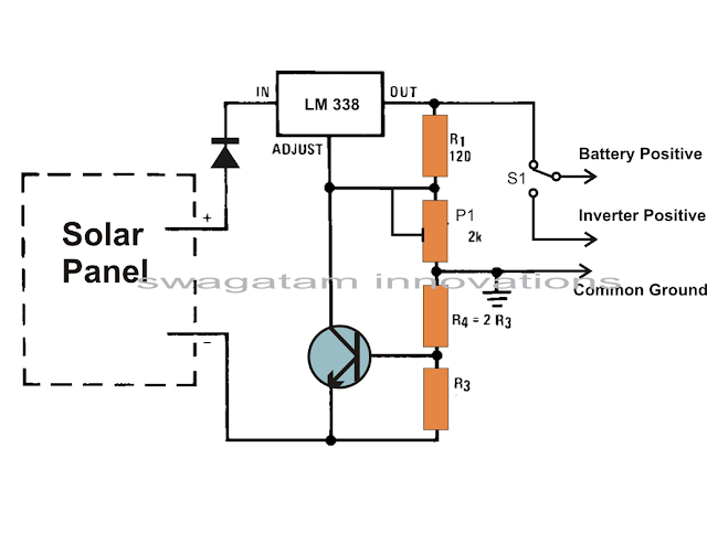
How to Build a Solar Panel Voltage Regulator Charger Circuit Charger Circuit at Home

How to Build a Solar Panel Voltage Regulator, Charger Circuit, Charger Circuit at Home


We all know pretty well about solar panels and their functions. The basic functions of these amazing devices is to convert solar energy or sun light into electricity.
Basically a solar panel is made up discrete sections of individual photo voltaic cells. Each of these cells are able to generate a tiny magnitude of electrical power, normally around 1.5 to 3 volts.  

Many of these cells over the panel are wired in series so that the total effective voltage generated by the entire unit mounts up to an usable 12 volts or 24 volts outputs.
The current generated by the unit is directly proportional to the level of the sun light incident over the surface of the panel.
The power generated from a solar panel is normally used for charging a lead acid battery. The lead acid battery when fully charged is used with an inverter for acquiring the required AC mains voltage for powering the house electrical.
Ideally the sun rays should be incident over the surface of the panel for it to function optimally. However since the sun is never still, the panel needs to track or follow the suns path constantly so that it generates electricity at an efficient rate.
 If you are interested to build an automatic dual tracker solar panel system you may refer one of my earlier articles. Without a solar tracker, the solar panel will be able to do the conversions only at around 30 % efficiency.
Coming back to our actual discussions about solar panels, this device may be considered the heart of the system as far converting solar energy into electricity is concerned, however the electricity generated requires a lot of dimensioning to be done before it can be used effectively in the preceding grid tie system.
The voltage acquired from a solar panel is never stable and varies drastically according to the position of the sun and intensity of the sun rays and of course on the degree of incidence over the solar panel.
This voltage if fed to the battery for charging can cause harm and unnecessary heating of the battery and the associated electronics; therefore can be dangerous to the whole system.
In order to regulate the voltage from the solar panel normally a voltage regulator circuit is used in between the solar panel output and the battery input. This circuit makes sure that the voltage from the solar panel never exceeds the safe value required by the battery for charging.
Normally to get optimum results from the solar panel, the minimum voltage output from the panel should be higher than the required battery charging voltage, meaning even during adverse conditions when the sun rays are not sharp or optimum, the solar panel still should be able to generate a voltage more than say 12 volts which may be the battery voltage under charge.
Solar Voltage regulators available in the market can be too costly and not so reliable; however making one such regulator at home using ordinary electronic components can be not only fun but also very economical.
Referring to the figure we see a circuit design that utilizes very ordinary components and yet fulfills the needs just as required by our specs.
 A single IC LM 338 becomes the heart of the entire configuration and becomes responsibly for implementing the desired voltage regulations single handedly.
The shown solar panel regulator, charger circuit is framed as per the standard mode of the IC 338 configuration.
The input is given to the shown input points of the IC and the output for the battery received at the output of the IC. The pot or the preset is used to accurately set the voltage level that may be considered as the safe value for the battery.
The circuit also offers a current control feature, which makes sure that the battery always receives a fixed predetermined charging current rate and is never over driven.
The module can be wired as directed in the diagram. The relevant positions indicated can be simply wired even by a layman. Rest of the function is taken care of by the regulator circuit.
The switch S1 should be toggled to inverter mode once the battery gets fully charged (as indicated over the meter).
The charging current may be selected by appropriately selecting the value of the resistors R3. It can be done by solving the formula:
0.6/R3 = 1/10 battery AH
The preset VR1 is adjusted for getting the required charging voltage from the regulator.
Continue Reading[...]

Sunday, March 31, 2013

How to Make a Simple Active Low Pass Filter Circuit Using IC 741


In electronics, filter circuits are basically employed for restricting the passage of a certain frequency range while allowing some other band of frequency into the further stages of the circuit.


Primarily there are three types of frequency filters that are used for the above mentioned operations.

These are: Low pass filter, high pass filter and the band pass filter.
 As the name suggests, a low pass filter circuit will allow all frequencies below a certain set frequency range.
A high pass filter circuit will allow only the frequencies which are higher than the preferred set range of frequency while a band pass filter will allow only an intermediate band of frequencies to flow to the next stage, inhibiting all frequencies which may be outside this set range of oscillations.

Filters are generally made with two types of configurations, the active type and the passive type.
Passive type filter are less efficient and involve complicated inductor and capacitor networks, making the unit bulky and undesirable. However these will not require any power requirement for itself to operate, a benefit too small to be considered really useful.
Contrary to this active type of filters are very efficient, can be optimized to the point and are less complicated in terms of component count and calculations.

In this article we are discussing a very simple circuit of a low pass filter, which was requested by one of our avid readers Mr.Bourgeoisie.

Looking at the circuit diagram we can see a very easy configuration consisting of a single opamp as the main active component.
The resistors and the capacitors are discretely dimensioned for a 50 Hz cut OFF, meaning no frequency above 50 Hz will be allowed to pass through the circuit into the output.
For technical explanation of the circuit you may refer to the data provided here.
Continue Reading[...]

Friday, March 29, 2013

The AM Transmitter Circuit for 500 KHz to 1600 KHz

This circuit is design for AM transmitter circuit. This circuit is operate for medium wave band for amplitude modulation. The operation of the circuit is in below.


The circuit is in two half, an audio amplifier and an RF oscillator. The oscillator is built around Q1 and associated components. The tank circuit L1 and VC1 is tunable from about 500 KHz to 1600 KHz. These components can be used from an old MW radio, if available. Q1 needs regenerative feedback to oscillate and this is achieved by connecting the base and collector of Q1 to opposite ends of the tank circuit. The 1nF capacitor C7, couples signals from the base to the top of L1, and C2, 100pF ensures that the oscillation is passed from collector, to the emitter, and via the internal base emitter resistance of the transistor, back to the base again. Resistor R2 has an important role in this circuit. It ensures that the oscillation will not be shunted to ground via the very low internal emitter resistance, re of Q1, and also increases the input impedance so that the modulation signal will not be shunted. Oscillation frequency is adjusted with VC1.

The Q2 is wired as a common emitter amplifier, C5 decoupling the emitter resistor and realizing full gain of this stage. The microphone is an electret condenser mic and the amount of AM modulation is adjusted with the 4.7k preset resistor P1. An antenna is not needed, but 30cm of wire may be used at the collector to increase transmitter range.
Continue Reading[...]

How to Understand and Use Transistors in Circuits

Transistors are the building blocks of all
semiconductor devices found today. If there wouldn’t be transistors
there wouldn’t be any ICs or any other semiconductor component. Even ICs
are made up of millions of closely knit transistors which constitute
the features of the particular chip.

New
electronic hobbyists usually find it difficult to handle these useful
components and configure them as circuits for an intended application.


Here we’ll study the functions and the way of handling and implementing bipolar transistors into practical circuits.

Bipolar
transistors are generally a three lead active electronic component
which fundamentally works as a switch for either switching ON or
switching OFF power to an external load or the following electronic
stage of the circuit.

Transistors
are normally recognized by their external package in which the
particular device may be embedded. The most common types of package in
which these useful devices are enclosed, are the T0-92, TO-126, TO-220
and TO-3. We will try to understand all these specifications of
transistors and also learn how to use them in practical circuits.

Understanding Small Signal TO-92 Transistors:

Transistors
like BC547, BC557, BC546, BC548, BC549, etc all come under this
category. These are the most elementary in the group and are used for
applications involving low voltages and currents. Interestingly this
category of transistors is used most extensively and universally in
electronic circuits due to their versatile parameters.

Normally these devices are designed to handle voltages anywhere between 30 to 60 volts across their collector and emitter.

The
base voltage is not more than 6, but they can be easily triggered with a
voltage level as low as 0.6 volts at their base. However the current
must be limited to 3 mA approximately.

The three leads of a TO-92 transistor may be identified in the following manner:

Keeping
the printed side toward us, the right side lead is the emitter, the
center one is the base and the left hand side leg is the collector of
the device.

How to Configure a TO-92 Transistor into Practical Circuit Designs

Transistors
are mainly of two types, an NPN type and a PNP type, both are
complementary to each other. Basically they both behave the same way but
in the opposite references and directions.

 For
example an NPN device will require a positive trigger with respect to
the ground while a PNP device will require a negative trigger with
reference to a positive supply line for implementing the specified
results.

The
three leads of the transistor explained above needs to be assigned with
specified inputs and outputs for making it work for a particular
application which obviously is for switching a parameter.

The leads need to be assigned with the following input and output parameters:

The
emitter of any transistor is the reference pin out of the device,
meaning it needs to be assigned the specified common supply reference so
that the remaining two leads can operate with reference to it. 

An
NPN transistor will always need a negative supply to be connected at
its emitter lead for functioning while for a PNP, a positive supply
line. The collector is the load carrying lead of a transistor and the
load which needs to be switched is introduced at the collector of a
transistor (see figure).

The
base of a transistor is the trigger terminal which is required to be
applied with a small voltage level so the current through the load can
pass through, across to the emitter line making the circuit complete and
operating the load. 

The
removal of the trigger supply to the base immediately switches OFF the
load or simply the current across the collector and the emitter
terminals.

Understanding TO-126, TO-220 Power Transistors:

These
are medium type of power transistors used for applications which
require switching of powerful relatively powerful loads lie
transformers, lamps etc. and for driving TO-3 devices, typical egs are
BD139, BD140, BD135 etc.


The pin out are identified in the following manner:

Holding
the device with its printed surface facing you, the right side lead is
the emitter, the center lead is the collector and the left side lead is
the base.

The functioning and the triggering principle is exactly similar to what is explained in the previous section.
The device is operated with loads anywhere from 100 mA to 2 amps across their collector to emitter.

The
base trigger can be anywhere from 1 to 5 volts with currents not
exceeding 50 mA depending upon the power of the loads to be switched.

Understanding TO-3 Power Transistors:

These
can be seen in metallic packages as shown in the figure. The common
examples of TO-3 power transistors are 2N3055, AD149, BU205, etc.


The leads of a TO-3 package can be identified as follows:

Holding
the lead side of the device toward you such that the metal part beside
the leads having larger area is held upward (see figure), the right side
lead is the base, the left side lead is the emitter while the metallic
body of the device forms the collector of the package.

The
function and operating principle is just about the same as explained
for the small signal transistor however the power specs increase
proportionately as given below:

Collector-emitter voltage can be anywhere between 30 to 400 volts and current between 10 to 30 Amps.
Base
trigger should be optimally around 5 volts, with current levels from 10
to 50 mA depending upon the magnitude of the load to be triggered. The
base triggering current is directly proportional to the load current.

Continue Reading[...]