Showing posts with label regulator. Show all posts
Showing posts with label regulator. Show all posts
Thursday, September 26, 2013
Discrete Voltage Regulator
The title of this article naturally raises the question of why we think that the generous selection of fully integrated voltage regulators needs to be extended with a version constructed using discrete components. In other words, what does this circuit offer that the well-known ‘three-leggers’ don’t have? To start with, we can point out that this circuit is refreshingly simple for a discrete version. Three semiconductors, three resistors, a capacitor and a diode are all it needs. Of course, that’s still more components than an integrated regulator, so what exactly are the advantages of this circuit?
 They are to be found in three areas: voltage range, bandwidth and current rating. The last of these is the primary strength of this circuit, since the maximum current depends only on the specifications of the output transistor. With the BD680, as used here, a current of 4 A can be delivered at a collect-emitter voltage of 10 V with adequate cooling (Rth = 3.12 K/W). The peak current is even 6 A. Try matching that with an integrated voltage regulator! The maximum input voltage is 30 V with the illustrated version of the circuit (UDSmax of T1), but this can easily be increased by using special high-voltage transistors.
 The same applies to the bandwidth, which can be extended as desired, without any modifications to the circuit, by using high-speed transistors. Generally speaking, wide bandwidth is also not one of the strong points of integrated voltage regulators. As noted, the circuit is basically very simple. A zener diode (D1) fed with a constant current of around 1mA by a JFET current source (T1) provides the reference potential. C1 is connected in parallel with D1 to provide well-behaved startup behaviour (soft start). This capacitor also provides additional buffering and decouples noise and other disturbances. The startup time is around three seconds.
The only additional item that is needed for the voltage regulator is an output buffer for the reference potential. This takes the form of a sort of super-Darlington using T2 and T3. This works very well, but has the disadvantage that the output voltage is a bit lower (one diode drop) than the Zener voltage. P1 can be added to correct this, but this does reduce the regulation of the circuit. If the voltage difference is not important, it is thus better to replace P1 with a wire jumper. The main specifications of the voltage regulator are listed in Table 1.
Continue Reading[...]
 They are to be found in three areas: voltage range, bandwidth and current rating. The last of these is the primary strength of this circuit, since the maximum current depends only on the specifications of the output transistor. With the BD680, as used here, a current of 4 A can be delivered at a collect-emitter voltage of 10 V with adequate cooling (Rth = 3.12 K/W). The peak current is even 6 A. Try matching that with an integrated voltage regulator! The maximum input voltage is 30 V with the illustrated version of the circuit (UDSmax of T1), but this can easily be increased by using special high-voltage transistors.
 The same applies to the bandwidth, which can be extended as desired, without any modifications to the circuit, by using high-speed transistors. Generally speaking, wide bandwidth is also not one of the strong points of integrated voltage regulators. As noted, the circuit is basically very simple. A zener diode (D1) fed with a constant current of around 1mA by a JFET current source (T1) provides the reference potential. C1 is connected in parallel with D1 to provide well-behaved startup behaviour (soft start). This capacitor also provides additional buffering and decouples noise and other disturbances. The startup time is around three seconds.
The only additional item that is needed for the voltage regulator is an output buffer for the reference potential. This takes the form of a sort of super-Darlington using T2 and T3. This works very well, but has the disadvantage that the output voltage is a bit lower (one diode drop) than the Zener voltage. P1 can be added to correct this, but this does reduce the regulation of the circuit. If the voltage difference is not important, it is thus better to replace P1 with a wire jumper. The main specifications of the voltage regulator are listed in Table 1.
Friday, May 17, 2013
MSK5012 Adjustable Voltage Regulator 10A

MSK5012 is a awful reliable adjustable voltage regulator.Whose achievement can be programmed application two resistors. The regulator has a actual low dropout voltage(0.45v @10A )due to the acceptance of MOSFT with actual low Rds (ON) as the centralized alternation canyon element.The MS5012 has a top akin of accurateness and ripple bounce is about 45dB. It is accessible in a 5 pin Sip amalgamation that is electrically abandoned from the centralized circuitry. This accord us the abandon to fit the IC anon to the calefaction bore and this array of absolute heatsinking improves the thermal dissipation.
The achievement voltage of this circuit is adjustable from 1.3v to 36v DC.Resistors R1 and R2 are acclimated for programming the achievement voltage. For all applications, amount of R2 is anchored to 10K. The accord amid R1,R2 and achievement voltage Vout is according to the blueprint R1=R2(Vout/1.235)-1. C1 is a clarify capacitor which is aswell a allotment of the aboideau drive circuit of the centralized alternation canyon MOSFET. About three times the ascribe voltage will arise beyond this capacitor and so the its voltage appraisement have to be called accordingly.C2 is the ascribe clarify capacitor while C3 is the achievement clarify capacitor.
Wednesday, April 10, 2013
Transistor Basic Voltage Regulator Circuit
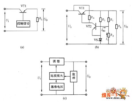 The transistors series voltage regulator circuit is shown in the picture. And, the picture (a) is equivalent circuit. The VT1 is adjustment transistor which is used to adjust the output voltage. The VT1 and load RL are in series. So this circuit is called the series voltage regulator circuit. Because the adjustment tube is using the transistors, the transistor series voltage regulator circuit could work under a big working current which could overcome the weakness that the zener diode regulator circuits output current is limited by the zener diode limiting current. The picture (b) is the practical series voltage regulator circuit. The picture (c) is its diagram circuit.
 Friday, April 5, 2013
How to Build a Solar Panel Voltage Regulator Charger Circuit Charger Circuit at Home
How to Build a Solar Panel Voltage Regulator, Charger Circuit, Charger Circuit at Home
We all know pretty well about solar panels and their functions. The basic functions of these amazing devices is to convert solar energy or sun light into electricity.
Basically a solar panel is made up discrete sections of individual photo voltaic cells. Each of these cells are able to generate a tiny magnitude of electrical power, normally around 1.5 to 3 volts.
Many of these cells over the panel are wired in series so that the total effective voltage generated by the entire unit mounts up to an usable 12 volts or 24 volts outputs.
The current generated by the unit is directly proportional to the level of the sun light incident over the surface of the panel.
The power generated from a solar panel is normally used for charging a lead acid battery. The lead acid battery when fully charged is used with an inverter for acquiring the required AC mains voltage for powering the house electrical.
Ideally the sun rays should be incident over the surface of the panel for it to function optimally. However since the sun is never still, the panel needs to track or follow the suns path constantly so that it generates electricity at an efficient rate.
If you are interested to build an automatic dual tracker solar panel system you may refer one of my earlier articles. Without a solar tracker, the solar panel will be able to do the conversions only at around 30 % efficiency.
Coming back to our actual discussions about solar panels, this device may be considered the heart of the system as far converting solar energy into electricity is concerned, however the electricity generated requires a lot of dimensioning to be done before it can be used effectively in the preceding grid tie system.
The voltage acquired from a solar panel is never stable and varies drastically according to the position of the sun and intensity of the sun rays and of course on the degree of incidence over the solar panel.
This voltage if fed to the battery for charging can cause harm and unnecessary heating of the battery and the associated electronics; therefore can be dangerous to the whole system.
In order to regulate the voltage from the solar panel normally a voltage regulator circuit is used in between the solar panel output and the battery input. This circuit makes sure that the voltage from the solar panel never exceeds the safe value required by the battery for charging.
Normally to get optimum results from the solar panel, the minimum voltage output from the panel should be higher than the required battery charging voltage, meaning even during adverse conditions when the sun rays are not sharp or optimum, the solar panel still should be able to generate a voltage more than say 12 volts which may be the battery voltage under charge.
Solar Voltage regulators available in the market can be too costly and not so reliable; however making one such regulator at home using ordinary electronic components can be not only fun but also very economical.
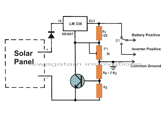
Referring to the figure we see a circuit design that utilizes very ordinary components and yet fulfills the needs just as required by our specs.
A single IC LM 338 becomes the heart of the entire configuration and becomes responsibly for implementing the desired voltage regulations single handedly.
The shown solar panel regulator, charger circuit is framed as per the standard mode of the IC 338 configuration.
The input is given to the shown input points of the IC and the output for the battery received at the output of the IC. The pot or the preset is used to accurately set the voltage level that may be considered as the safe value for the battery.
The circuit also offers a current control feature, which makes sure that the battery always receives a fixed predetermined charging current rate and is never over driven.
The module can be wired as directed in the diagram. The relevant positions indicated can be simply wired even by a layman. Rest of the function is taken care of by the regulator circuit.
The switch S1 should be toggled to inverter mode once the battery gets fully charged (as indicated over the meter).
The charging current may be selected by appropriately selecting the value of the resistors R3. It can be done by solving the formula:
0.6/R3 = 1/10 battery AH
The preset VR1 is adjusted for getting the required charging voltage from the regulator.
Thursday, April 4, 2013
Simple Current Regulator Circuit Using LM10

The current regulator is a bit unusual in that the supply current of the IC flows through the sense resistor and does not affect accuracy as long as it is less than the desired output current. It is also possible to use remote amplifiers with two-wire signal transmission, as was done with the comparators. Remote sensors can be particularly troublesome when low-level analog signals are involved. Transmission problems include induced noise, ground currents, shunting from cable capacitance, resistance drops and thermoelectric potentials. These problems can be largely eliminated by amplifying the signal at the source and altering impedances to levels more suitable for transmission. Here is a schematic drawing :
Subscribe to:
Comments (Atom)